What is a Fine Line PCB?
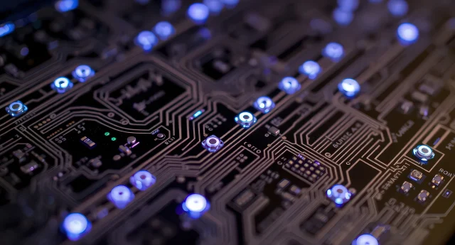
A Fine Line PCB is a printed circuit board designed with extremely narrow trace widths and spacing, typically below 100 microns. These PCBs are essential for high-density electronic designs where space is limited and performance requirements are demanding.
Fine line technology is widely used in applications that require compact layouts, high pin-count components, and high-speed signal transmission. Compared to standard PCBs, fine line boards offer increased routing density, enabling designers to integrate more functionality within a smaller footprint.
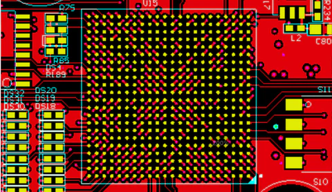
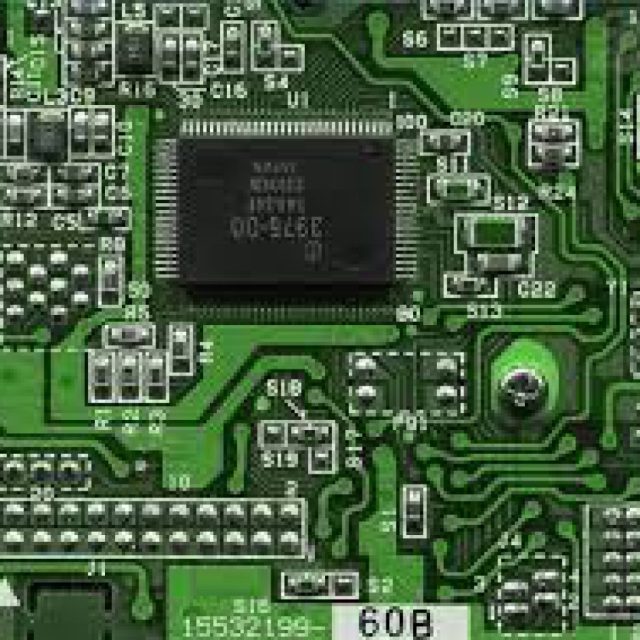
Fine line PCBs are often associated with advanced technologies such as HDI (High-Density Interconnect), microvia structures, and fine-pitch components like BGA and CSP packages.
Fine Line PCB Design
Designing fine line PCBs requires precision and careful optimization across multiple aspects:
-
Trace Width and Spacing Control:
The defining feature of fine line PCBs is ultra-narrow traces and spacing. Designers must carefully calculate tolerances to ensure manufacturability while maintaining electrical performance. Even minor deviations can result in shorts or open circuits. -
Signal Integrity Optimization:
With tighter routing, signal interference becomes more likely. Controlled impedance design, differential pair routing, and proper grounding strategies are essential to minimize crosstalk and signal degradation, especially in high-speed applications. -
Layer Stack-Up and Routing Density:
Multilayer stack-ups are typically used to support high routing density. Strategic layer allocation for signal, power, and ground helps maintain performance while maximizing available routing space. -
Via Strategy and Microvias:
Fine line PCBs often incorporate microvias, blind vias, or buried vias to enable efficient interconnection without consuming excessive surface area. Staggered or stacked via designs can further enhance routing flexibility. -
Material Selection:
High-performance laminates with stable dielectric properties are preferred to maintain signal integrity and dimensional stability during fabrication. Low-loss materials may also be used in high-frequency designs.
Manufacturing Considerations and QA
Producing fine line PCBs is one of the most demanding processes in PCB fabrication, requiring strict process control and advanced equipment:
-
High-Precision Imaging and Etching: Advanced photolithography ensures accurate pattern transfer for ultra-fine traces. Etching processes must be tightly controlled to avoid undercutting or over-etching.
-
Cleanroom Environment: Fine line production requires contamination-free environments to prevent defects that could compromise narrow traces.
-
Advanced Solder Mask Application: Precise solder mask alignment is critical to prevent bridging between fine pads.
-
Laser Drilling and Microvia Formation: High-accuracy laser drilling ensures reliable microvia structures in dense layouts.
Quality assurance plays a crucial role in ensuring reliability:
-
Automated Optical Inspection (AOI): Detects fine trace defects, opens, or shorts.
-
X-ray Inspection: Verifies internal structures such as vias and multilayer alignment.
-
Electrical Testing: Ensures continuity and impedance compliance.
-
Cross-Section Analysis: Confirms trace geometry and layer integrity.
KKPCB applies these advanced manufacturing and QA processes to consistently deliver high-yield fine line PCBs for demanding applications.
Applications of Fine Line PCBs
Fine line PCBs are essential in industries where miniaturization and performance are critical:
-
Smartphones and Wearable Devices: Supporting compact, high-functionality designs.
-
High-Speed Computing and Data Centers: Enabling dense routing for processors and memory modules.
-
Automotive Electronics: Powering ADAS, infotainment systems, and sensor integration.
-
Industrial IoT and Embedded Systems: Delivering compact, high-performance control and communication modules.
As electronics continue to evolve toward higher density and performance, fine line PCB technology will remain a key enabler. With expertise in precision fabrication, advanced materials, and rigorous quality control, KKPCB provides fine line PCB solutions that meet the most demanding industry requirements.
