What is a Microvia PCB?
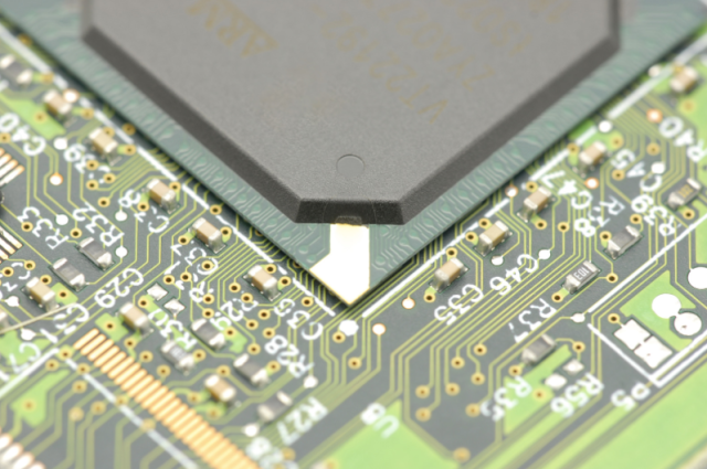
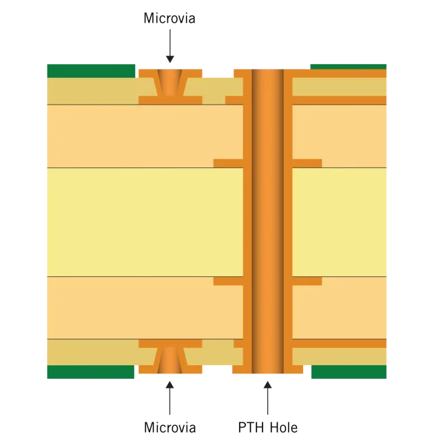
A Microvia PCB is a printed circuit board that uses very small vias—typically less than 150 microns in diameter—to connect adjacent layers. Unlike traditional through-hole or buried vias, microvias enable high-density routing and reduced signal path lengths, making them ideal for high-speed, high-performance, and compact electronic designs.
Microvia technology is widely used in:
-
High-density interconnect (HDI) boards
-
Mobile devices and wearables
-
RF and high-speed digital applications
Microvia PCB Design
Designing microvia PCBs requires careful consideration of layout, layer stack-up, and signal integrity:
-
Layer Stack-Up Optimization:
Microvias are typically used to connect only adjacent layers. Designers often implement stacked or staggered microvias to maximize routing efficiency while minimizing parasitic inductance. Proper stack-up also improves power distribution and signal integrity. -
Fine Line and Space Routing:
Microvia PCBs allow very fine trace widths and spacing, enabling compact component placement. Controlled impedance and differential pair routing are essential for high-speed digital signals and RF circuits. -
Thermal Management:
Microvias can double as thermal vias, transferring heat from inner layers to outer layers. Proper placement ensures efficient heat dissipation and reduces hotspots, which is crucial for high-power devices. -
Material Selection:
Low-loss laminates and high-Tg materials are used to maintain signal integrity and reliability during thermal cycling. Advanced substrates like Rogers or hybrid FR-4 composites are often selected for high-frequency applications.
Manufacturing Considerations and QA
Producing microvia PCBs is more complex than standard multilayer boards and requires advanced fabrication techniques:
-
Laser Drilling: High-precision laser drilling is used to create microvias with diameters typically under 150 microns.
-
Sequential Lamination: Layers are laminated in stages to accommodate microvias and maintain alignment.
-
Via Filling and Plating: Copper-filled or plated microvias enhance electrical performance, mechanical stability, and thermal conductivity.
-
Inspection and Testing: AOI, X-ray inspection, electrical testing, and thermal cycling are performed to ensure connectivity, impedance consistency, and overall reliability.
KKPCB leverages these processes to produce microvia PCBs that meet demanding electrical, thermal, and mechanical requirements.
Applications of Microvia PCBs
Microvia PCBs are critical in applications requiring high-density, high-speed, and high-performance designs:
-
Mobile Devices and Wearables: Enabling compact designs with high-pin-count ICs.
-
HDI and High-Speed Computing: Supporting signal-intensive processors, memory, and networking modules.
-
Automotive and ADAS Electronics: Ensuring reliability and compactness for ECUs and sensor modules.
-
RF and 5G Modules: Reducing signal path length and maintaining integrity for high-frequency communication devices.
By integrating precise design, advanced materials, sophisticated fabrication, and rigorous testing, KKPCB delivers microvia PCBs that provide the performance, density, and reliability required for modern electronics.
