Millimeter-wave (mmWave) technology is a key component of modern wireless communication and sensing systems. Operating at frequencies typically ranging from 24 GHz to 100 GHz, mmWave technology enables ultra-high data transmission speeds, improved bandwidth, and high-resolution radar detection.
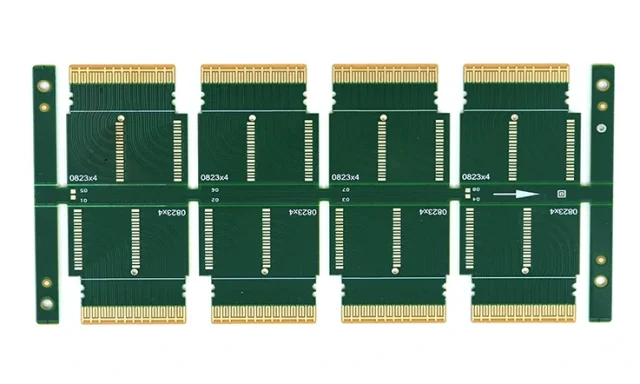
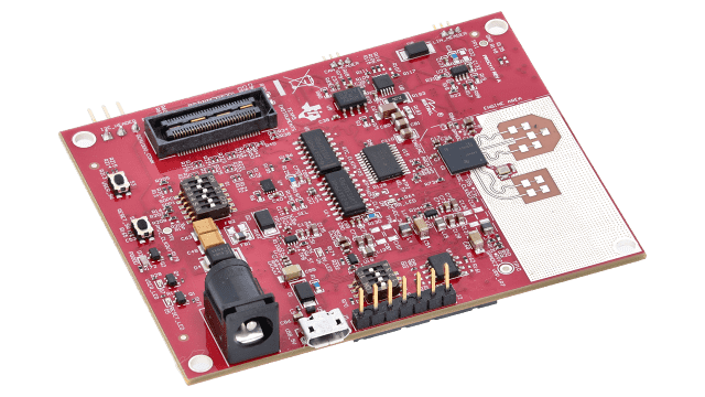
At the core of these systems is the mmWave Module PCB, a specialized circuit board designed to handle extremely high-frequency signals with minimal loss. These PCBs integrate RF front-end circuits, antennas, power amplifiers, and signal processing components within compact modules.
What is an mmWave Module PCB?
An mmWave Module PCB is a high-frequency printed circuit board specifically engineered for millimeter-wave signal transmission.
These PCBs are commonly used in compact RF modules that integrate:
-
RF transceivers
-
Antenna arrays
-
Power amplifiers
-
Signal processing circuits
Because mmWave signals are highly sensitive to material properties and layout accuracy, PCB design and fabrication must meet extremely tight tolerances.Key Design Requirements for mmWave Module PCB
Key Design Requirements for mmWave Module PCB
1. Ultra-Low Loss PCB Materials
Millimeter-wave frequencies are very sensitive to dielectric loss. To maintain signal quality, designers typically use specialized RF materials such as:
-
Low-loss PTFE substrates
-
Hydrocarbon ceramic laminates
-
High-frequency RF laminates
These materials provide stable dielectric constants and minimal signal attenuation at very high frequencies.
2. Precise Impedance Control
Maintaining precise impedance across RF transmission lines is critical for mmWave circuits.
Key design practices include:
-
Controlled impedance microstrip or stripline routing
-
Accurate trace width and spacing
-
Proper impedance matching between components
These measures reduce signal reflections and improve RF transmission efficiency.
3. Compact Multilayer PCB Structure
mmWave modules often integrate multiple high-frequency circuits in a compact footprint.
Multilayer PCB designs help achieve:
-
Efficient signal routing
-
Improved ground shielding
-
Reduced electromagnetic interference
Advanced PCB technologies such as HDI structures and microvias are commonly used to support dense mmWave module layouts.
4. Antenna Integration
Many mmWave modules integrate antenna-on-PCB or antenna-in-package (AiP) structures.
PCB designers must carefully optimize:
-
Antenna placement
-
Ground plane design
-
Radiation efficiency
This ensures optimal wireless signal performance and coverage.
5. Thermal Management
High-frequency RF components such as power amplifiers generate heat during operation.
Effective thermal design techniques include:
-
Thermal vias
-
Copper heat spreading layers
-
Optimized component placement
Proper thermal management improves reliability and extends module lifespan.
Applications of mmWave Module PCB
mmWave module PCBs are widely used in advanced wireless technologies, including:
-
5G millimeter-wave base stations
-
Automotive radar systems (77 GHz / 79 GHz)
-
High-speed wireless communication devices
-
Satellite communication systems
-
Advanced driver assistance systems (ADAS)
These applications require extremely high signal integrity and reliable RF performance.
Manufacturing Challenges of mmWave PCB
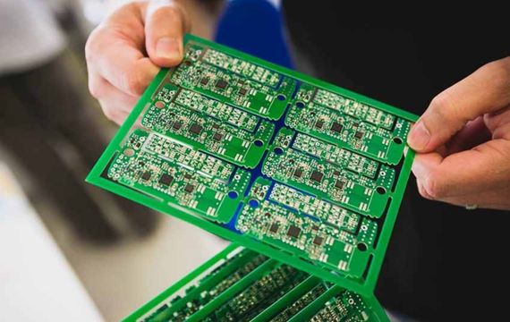
Producing mmWave module PCBs requires advanced manufacturing capabilities, including:
-
Precision impedance control
-
Fine line and spacing fabrication
-
Accurate multilayer lamination
-
Processing of high-frequency materials
Strict quality control and RF testing are essential to ensure consistent performance at millimeter-wave frequencies.
Conclusion
As technologies such as 5G communication, automotive radar, and high-speed wireless systems continue to evolve, the importance of high-performance mmWave Module PCBs continues to grow.
By combining ultra-low loss materials, precise RF design techniques, and advanced manufacturing processes, mmWave module PCBs provide the foundation for next-generation high-frequency electronic systems.
