Introduction to Multilayer HF PCB
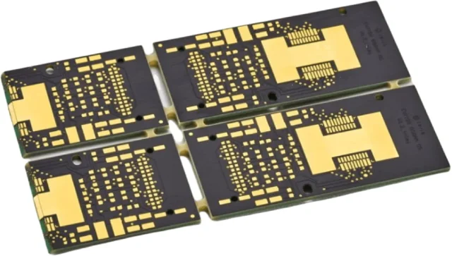
With the rapid advancement of wireless communication, radar systems, and high-speed electronics, the demand for Multilayer HF PCB (High-Frequency PCB) technology continues to grow. A Multilayer HF PCB is designed to support high-frequency signal transmission while integrating multiple circuit layers into a compact structure.
Compared with traditional PCB designs, multilayer high-frequency PCBs provide better signal integrity, improved electromagnetic shielding, and higher routing density. These features make them essential for modern RF systems, microwave circuits, and high-speed communication equipment.
What Is a Multilayer HF PCB?
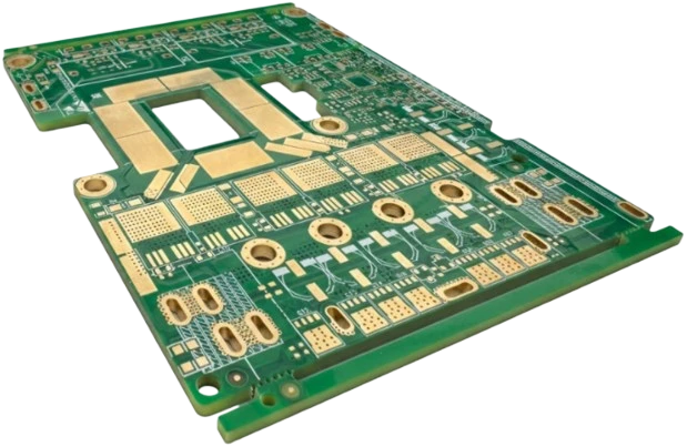
A Multilayer HF PCB is a high-frequency printed circuit board composed of multiple conductive layers separated by specialized dielectric materials optimized for RF and microwave signals.
These boards combine high-frequency PCB materials with multilayer PCB structures to support complex circuit routing and stable signal transmission at GHz-level frequencies.
Typical characteristics of multilayer HF PCBs include:
-
Multiple copper layers for high-density routing
-
Low-loss high-frequency laminate materials
-
Controlled impedance transmission lines
-
Strong electromagnetic shielding between layers
These features allow multilayer HF PCBs to maintain excellent electrical performance in demanding high-frequency applications.
Advantages of Multilayer HF PCB
1. Superior Signal Integrity
A well-designed multilayer HF PCB minimizes signal loss, crosstalk, and electromagnetic interference, ensuring stable RF signal transmission.
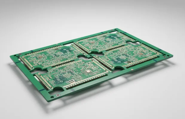
2. High-Density Circuit Integration
Multilayer structures enable engineers to integrate complex RF circuits and digital control systems within a compact PCB layout.
3. Enhanced Electromagnetic Shielding
Ground planes and power planes in multilayer high-frequency PCBs help reduce interference and improve overall circuit stability.
4. Improved Thermal Management
Multiple copper layers and optimized stackups help distribute heat effectively in high-frequency electronic systems.
5. Reliable Controlled Impedance
Precise stackup design allows accurate impedance control for microstrip lines, stripline routing, and other RF transmission structures.
Materials Used in Multilayer HF PCB
Selecting the right high-frequency PCB materials is essential for multilayer HF PCB fabrication. These materials must have low dielectric loss, stable dielectric constant, and excellent thermal performance.
High-frequency laminate materials from companies such as Rogers Corporation are commonly used in RF and microwave PCB designs due to their superior electrical properties.
Other commonly used materials include PTFE-based laminates and ceramic-filled RF substrates.
Design Considerations for Multilayer HF PCB
Designing a reliable Multilayer HF PCB requires careful attention to several key engineering aspects:
Controlled Impedance Routing
Accurate impedance control is critical for maintaining signal integrity in high-frequency circuits.
Optimized PCB Stackup
A well-planned multilayer stackup ensures proper signal isolation, stable grounding, and reduced electromagnetic interference.
Low-Loss Transmission Lines
Design techniques such as microstrip and stripline routing help maintain signal quality at high frequencies.
Via and Transition Optimization
Reducing unnecessary vias and optimizing signal transitions help minimize insertion loss and signal reflection.
Applications of Multilayer HF PCB
Multilayer HF PCBs are widely used in advanced electronic systems requiring high-frequency signal processing, including:
-
RF communication systems
-
5G base station equipment
-
Microwave communication modules
-
Automotive radar systems
-
Satellite communication hardware
-
Aerospace electronic systems
These applications rely on high-frequency multilayer PCB technology to maintain stable performance at high operating frequencies.
Manufacturing Requirements
Fabricating multilayer HF PCBs requires advanced PCB manufacturing technologies and strict process control, including:
-
Precision multilayer PCB lamination
-
High-frequency laminate processing
-
Controlled impedance manufacturing
-
Low surface roughness copper foil
-
Advanced surface finishes such as ENIG or immersion silver
These manufacturing processes ensure that multilayer HF PCBs meet the strict performance requirements of RF and microwave electronics.
Conclusion
Multilayer HF PCB technology is essential for modern high-frequency electronic systems. By combining advanced high-frequency PCB materials, optimized multilayer stackup designs, and precise controlled impedance routing, engineers can build reliable circuit boards capable of supporting RF, microwave, and high-speed communication applications.
As wireless communication and radar technologies continue to evolve, multilayer HF PCBs will remain a critical foundation for next-generation high-frequency electronics.
