What Is a High Speed PCB?
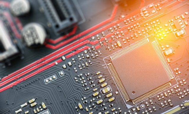
A High Speed PCB is a printed circuit board engineered to support high-frequency digital signals and rapid data transmission while maintaining signal integrity and stable electrical performance.
In modern electronics, devices such as servers, networking equipment, and communication systems operate with very fast switching speeds and multi-gigabit data rates. Under these conditions, PCB traces behave more like transmission lines than simple electrical connections. This makes careful PCB design essential to prevent signal distortion, timing errors, and electromagnetic interference.
High Speed PCBs are widely used in:
-
Data centers and high-performance computing systems
-
Telecommunications infrastructure
-
High-speed networking devices
-
Medical imaging equipment
-
Advanced industrial control systems
Proper design ensures that high-speed signals can travel across the board without significant loss, reflection, or interference.
Key Characteristics of High Speed PCB
High Speed PCBs differ from standard circuit boards in several important ways.
Controlled Impedance Routing
Maintaining consistent impedance along signal paths is critical for high-speed circuits. Proper impedance control helps prevent signal reflections and ensures reliable data transmission.
Signal Integrity Optimization
High speed signals are sensitive to distortion. PCB designers must manage:
-
Crosstalk between adjacent traces
-
Signal reflections
-
Propagation delay
-
Timing skew
Careful layout and routing techniques help maintain clean signal waveforms.
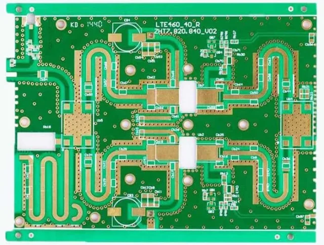
Multilayer Stack-Up Structure
Most high speed PCBs use multilayer stack-ups to provide dedicated ground and power planes. These planes improve signal return paths and reduce electromagnetic interference.
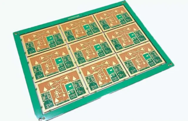
High Performance Materials
In many high-speed designs, specialized materials with low dielectric loss and stable dielectric constant are used to support high-frequency signal transmission.
Important Design Considerations
Designing a reliable high-speed PCB requires careful planning across multiple aspects of the board.
PCB Stack-Up Planning
A well-designed stack-up structure ensures stable impedance and efficient signal routing. Designers typically include multiple ground layers to improve signal reference and reduce noise.
Trace Length Matching
In high-speed digital interfaces, signals must often arrive at the same time. Length matching techniques are used to minimize timing skew between signal pairs or data buses.
Differential Pair Routing
Many high-speed interfaces use differential signaling to reduce noise and improve signal quality. Proper spacing and symmetry between differential pairs are critical.
Power Integrity
High-speed devices require stable power delivery. Designers must ensure proper decoupling capacitor placement and low impedance power distribution networks.
Applications of High Speed PCB
High Speed PCBs are essential in many advanced electronic systems where fast data transfer is required.
Common applications include:
-
High-speed communication equipment
-
Data center servers and storage systems
-
Network switches and routers
-
Automotive advanced driver assistance systems (ADAS)
-
High-speed test and measurement equipment
These systems depend on reliable PCB design to support multi-gigabit data transmission and stable system operation.
Conclusion
A High Speed PCB plays a critical role in modern electronics that demand fast and reliable data communication. Through careful design techniques such as controlled impedance routing, multilayer stack-up planning, and signal integrity optimization, high-speed PCBs ensure stable performance in demanding applications.
As data rates continue to increase across industries, high-speed PCB technology will remain essential for enabling next-generation electronic systems.
