What Is a Satellite PCB?
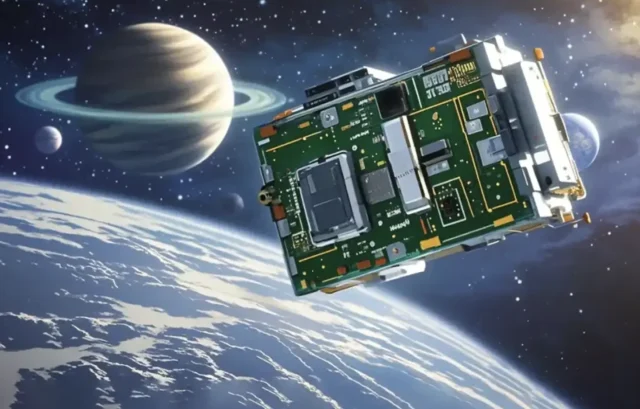
A Satellite PCB is a specialized printed circuit board designed for satellite systems and aerospace communication equipment. These PCBs must operate reliably in extreme environments, including high radiation, vacuum conditions, and significant temperature fluctuations.
Satellite PCBs support critical electronic functions such as:
-
Satellite communication modules
-
Signal processing systems
-
Power management units
-
Navigation and telemetry systems
Because satellite electronics cannot be easily repaired once deployed, the PCB design must ensure maximum reliability, durability, and long-term stability.
Key Design Requirements for Satellite PCB
1. High Reliability and Long-Term Stability
Satellite systems require electronics that can operate continuously for many years without failure. PCB design must therefore focus on:
-
High-quality materials with excellent stability
-
Strict manufacturing tolerances
-
Advanced inspection and testing procedures
These measures ensure the PCB maintains consistent electrical performance throughout the satellite’s operational lifespan.
2. Resistance to Extreme Temperature Conditions
Satellites experience large temperature variations when moving between sunlight and shadow in orbit. Satellite PCBs must withstand extreme thermal cycling without performance degradation.
Common design considerations include:
-
High TG materials
-
Thermal management layers
-
Carefully balanced multilayer stack-ups
These features help maintain structural integrity and prevent warpage or signal instability.
3. High-Frequency Signal Performance
Satellite communication systems often operate at microwave or high-frequency bands. PCB design must support:
-
Controlled impedance routing
-
Low-loss dielectric materials
-
Optimized RF trace layouts
These techniques minimize signal loss and maintain clear communication signals between satellites and ground stations.
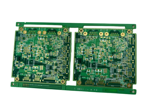
4. Multilayer and High-Density Design
Satellite electronics integrate numerous subsystems within a limited space. Multilayer PCB structures allow:
-
Complex signal routing
-
Dedicated power and ground planes
-
Reduced electromagnetic interference (EMI)
High-density PCB design improves system integration while maintaining signal integrity.
5. Radiation and Environmental Resistance
Space environments expose electronics to cosmic radiation and vacuum conditions. Satellite PCBs are designed to withstand:
-
Radiation exposure
-
Mechanical vibration during launch
-
Outgassing in vacuum environments
Using specialized materials and manufacturing processes ensures the board remains stable and reliable in space conditions.
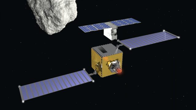
Applications of Satellite PCB
Satellite PCBs are widely used in aerospace and communication systems, including:
-
Communication satellites
-
Earth observation satellites
-
Navigation systems (GNSS)
-
Satellite payload electronics
-
Ground station communication equipment
These applications require PCBs that deliver high signal performance and long-term reliability.
Satellite PCB vs Standard PCB
| Feature | Standard PCB | Satellite PCB |
|---|---|---|
| Reliability Requirement | Moderate | Extremely high |
| Operating Environment | Normal | Space / extreme conditions |
| Frequency Performance | Standard | High-frequency RF support |
| Temperature Resistance | Standard | Extreme thermal cycling |
| Testing Standards | General | Aerospace-level testing |
Satellite PCBs are engineered for mission-critical performance where failure is not acceptable.
Conclusion
A Satellite PCB is a highly specialized circuit board designed for aerospace and satellite communication systems. With advanced materials, controlled impedance routing, multilayer structures, and resistance to extreme environmental conditions, these PCBs provide the reliability required for long-term space missions.
As satellite technology continues to expand in areas such as global communication, navigation, and Earth observation, high-performance satellite PCBs remain a key component enabling reliable space electronics.
