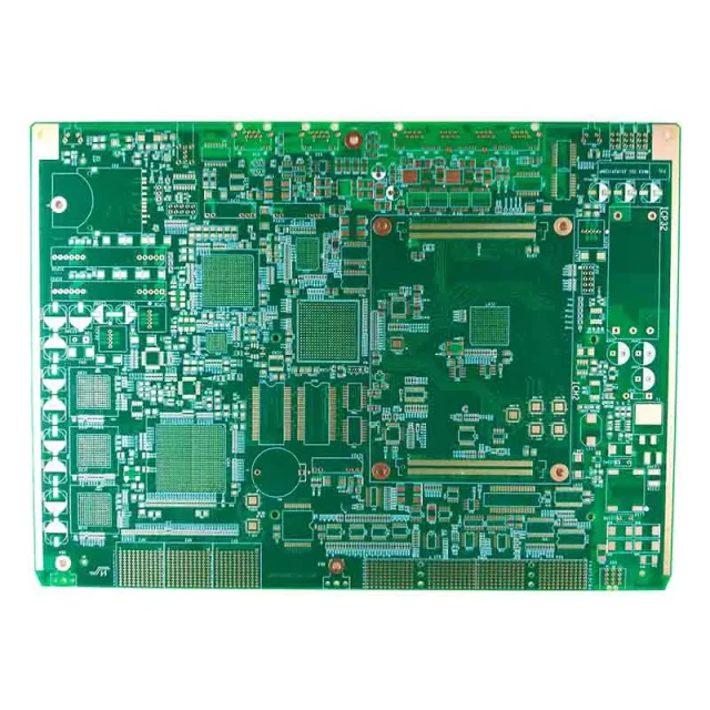
What Is a Multilayer HF PCB?
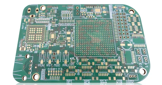
A Multilayer HF PCB is a high-frequency printed circuit board constructed with multiple conductive layers and low-loss dielectric materials to support RF and microwave signal transmission.
Unlike standard multilayer boards, multilayer HF PCBs are engineered specifically for GHz-level operation, where signal integrity, dielectric stability, and insertion loss control become critical design factors.
These boards are commonly used in:
-
5G communication equipment
-
RF power amplifiers
-
Radar modules
-
Satellite communication systems
-
High-frequency sensor platforms
Why Multilayer Structure Matters in High-Frequency Design
High-frequency circuits often require:
-
Dedicated ground reference layers
-
Isolated RF routing layers
-
Shielded power distribution layers
-
Controlled impedance signal paths
A multilayer stack-up allows engineers to:
-
Reduce electromagnetic interference (EMI)
-
Improve signal isolation
-
Optimize return current paths
-
Increase routing density
Proper layer allocation significantly improves RF stability and overall system performance.
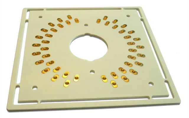
Material Selection for Low-Loss Performance
In high-frequency PCB design, dielectric loss directly impacts signal strength and efficiency.
Multilayer HF PCBs typically use advanced laminates supplied by companies such as Rogers Corporation or Taconic.
Key material properties include:
-
Low dielectric constant (Dk)
-
Low dissipation factor (Df)
-
Stable dielectric performance across temperature
-
Consistent impedance characteristics
In many designs, hybrid stack-ups combine RF laminate with high-TG FR4 to balance cost and performance.
Controlled Impedance and Signal Integrity
Maintaining consistent impedance is essential for RF transmission lines.
Design techniques include:
-
Microstrip and stripline structures
-
Tight trace width tolerance
-
Differential pair matching
-
Via transition optimization
-
Back-drilling for stub removal
Even small variations in trace geometry or dielectric thickness can cause signal reflection and performance degradation at high frequencies.
Thermal and Mechanical Stability
High-frequency modules often operate under high power density. Multilayer HF PCBs must provide:
-
Thermal via arrays
-
Copper plane heat spreading
-
Balanced stack-up to prevent warpage
-
Low CTE materials for dimensional stability
Thermal management ensures long-term reliability and stable RF characteristics.
Manufacturing Considerations
Producing multilayer HF PCBs requires strict process control:
-
Accurate lamination pressure and temperature
-
Tight dielectric thickness tolerance
-
Precise drilling and plating control
-
Surface finish selection optimized for RF performance
Surface finishes such as ENIG or immersion silver are often chosen to maintain consistent high-frequency signal behavior.
Applications of Multilayer HF PCB
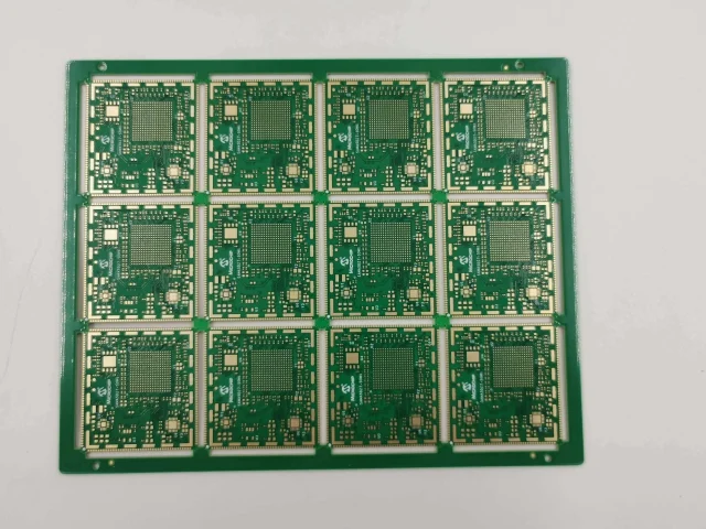
Multilayer HF PCBs are widely used in:
-
5G base station RF boards
-
Microwave communication modules
-
Automotive radar systems
-
Satellite transceivers
-
Industrial RF monitoring equipment
As wireless bandwidth increases, multilayer high-frequency PCB complexity continues to grow.
Multilayer HF PCB vs Standard Multilayer PCB
| Feature | Standard Multilayer PCB | Multilayer HF PCB |
|---|---|---|
| Frequency Range | Low–Medium | High (GHz-level) |
| Dielectric Material | FR4 | Low-Loss RF Laminate |
| Signal Loss Control | Moderate | Critical |
| EMI Management | Basic | Advanced |
| Manufacturing Tolerance | Standard | Tight |
Multilayer HF PCBs are engineered for precision RF performance and long-term stability.
Conclusion
A Multilayer HF PCB provides the structural and electrical foundation required for high-frequency RF systems.
Through low-loss materials, optimized stack-up design, controlled impedance routing, and strict manufacturing control, these boards enable reliable high-speed signal transmission across demanding applications.
As wireless and radar technologies continue advancing, multilayer high-frequency PCB design remains essential for achieving stable, efficient, and scalable RF performance.
