What Is a 5G Router PCB?
A 5G Router PCB is a high-performance printed circuit board designed to support ultra-fast wireless data transmission, multi-antenna systems, and high-speed signal processing in 5G networking devices.
Unlike traditional router boards, 5G router PCBs must handle:
-
Sub-6 GHz and mmWave frequencies
-
High-speed digital interfaces
-
Dense RF front-end integration
-
Continuous thermal load
This requires advanced PCB materials, controlled impedance routing, and optimized multilayer stack-up design.
Key Technical Requirements
1. High-Speed Signal Integrity
5G routers process massive data streams via:
-
High-speed Ethernet (2.5G/5G/10G)
-
PCIe interfaces
-
DDR memory buses
-
RF transceiver modules
To maintain signal integrity, the PCB must include:
-
Precise impedance control
-
Low-loss dielectric materials
-
Differential pair routing
-
Minimized crosstalk
Stable signal transmission is critical for maintaining low latency and high throughput.
2. RF Performance and Antenna Integration
Modern 5G routers integrate:
-
Multiple-input multiple-output (MIMO) antenna arrays
-
RF power amplifiers
-
Low-noise amplifiers (LNA)
-
RF filters and matching networks
To support high-frequency RF circuits, designers often use low-loss materials from manufacturers such as Rogers Corporation or Taconic.
Proper RF layout includes:
-
Short RF trace routing
-
Solid ground planes
-
Controlled via transitions
-
EMI shielding strategies
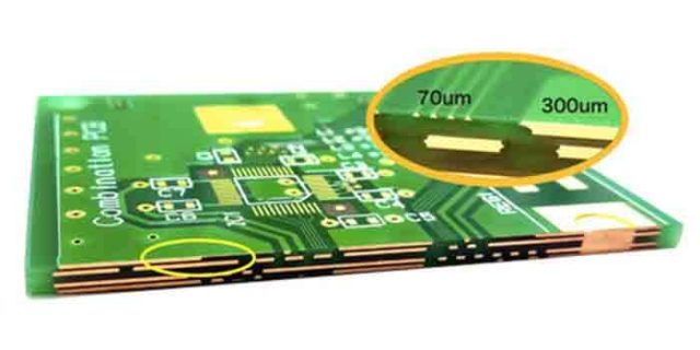
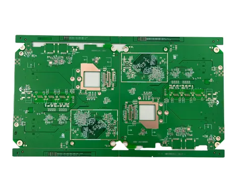
3. Multilayer and HDI Structure
5G router PCBs typically use:
-
6–16 layers or more
-
HDI structures with microvias
-
Dedicated RF layers
-
Power and ground plane separation
This multilayer architecture supports:
-
Dense component placement
-
Improved EMI control
-
Optimized signal isolation
HDI technology allows compact form factors without sacrificing performance.
4. Thermal Management
5G chipsets and RF power modules generate significant heat. Effective thermal design includes:
-
Heavy copper layers
-
Thermal vias under power components
-
Copper planes for heat spreading
-
Heat sink integration
Reliable heat dissipation ensures long-term stability and prevents signal degradation.
5. Power Distribution Stability
5G routers require stable and clean power for:
-
Baseband processors
-
RF modules
-
High-speed memory
-
Network switching ICs
A well-designed PCB includes:
-
Low-impedance power planes
-
Decoupling capacitor optimization
-
Controlled return paths
This guarantees consistent device performance.
Applications of 5G Router PCB
-
Home and enterprise 5G routers
-
Industrial 5G gateways
-
Outdoor CPE devices
-
Smart city networking equipment
-
Fixed wireless access (FWA) systems
These applications demand high reliability and stable wireless connectivity.
5G Router PCB vs Traditional Router PCB
| Feature | Traditional Router PCB | 5G Router PCB |
|---|---|---|
| Frequency Range | < 6 GHz | Sub-6 GHz & mmWave |
| Layer Count | 4–8 layers | 6–16+ layers |
| Material | FR4 | Low-loss + Hybrid |
| Thermal Design | Moderate | Advanced |
| Data Speed | Moderate | Ultra-High |
5G router PCBs are engineered for higher bandwidth, lower latency, and stronger RF performance.
Conclusion
A 5G Router PCB is a sophisticated multilayer board designed to support high-frequency RF circuits, high-speed digital interfaces, and advanced thermal management.
With controlled impedance routing, HDI structures, and optimized RF design, 5G router PCBs enable reliable next-generation wireless communication.
For manufacturers developing high-performance networking devices, a well-designed 5G router PCB is essential for ensuring stable connectivity, high throughput, and long-term durability.
