What Is a 5G Router PCB?
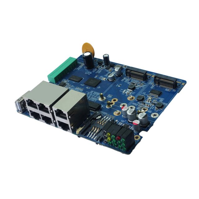
A 5G Router PCB is a printed circuit board specifically designed for 5G wireless routers and communication devices. Unlike standard PCB designs, 5G router PCBs must handle multi-GHz signals, support MIMO antenna arrays, and maintain signal integrity in high-density multilayer designs.
These PCBs enable ultra-fast data transmission, low latency, and reliable network connectivity in both consumer and industrial 5G applications.
Key Design Features
1. High-Frequency Performance
5G signals operate in sub-6 GHz and mmWave bands (24–52 GHz). PCB materials and trace designs must minimize:
-
Signal attenuation
-
Insertion loss
-
Crosstalk
Low-loss laminates such as RO4350B, RF-35, or Taconic high-frequency materials are commonly used.
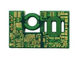
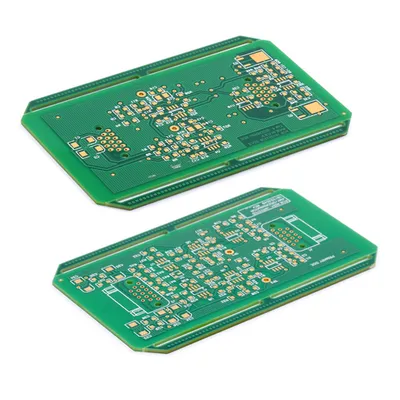
2. Multilayer Stack-Up
5G router PCBs often feature 6–10 layers to accommodate:
-
RF signal layers
-
Ground planes for shielding
-
Power distribution planes
-
Digital control and interface layers
A carefully designed stack-up ensures controlled impedance and reduces electromagnetic interference (EMI).
3. MIMO and Antenna Integration
5G routers rely on multi-input multi-output (MIMO) antennas for high-speed connectivity. PCB design must support:
-
Proper RF trace routing
-
Low-loss signal paths to antennas
-
Shielding between multiple RF channels
This allows high throughput and minimal signal degradation.
4. Thermal Management
High-speed 5G modules generate significant heat due to:
-
RF power amplifiers
-
High-speed processors
-
Network switching ICs
PCB design uses thick copper planes, thermal vias, and heat-spreading layers to ensure reliable operation.
5. Signal Integrity and EMI Control
Maintaining signal integrity is crucial in dense 5G PCB layouts. Techniques include:
-
Segregation of analog, digital, and RF traces
-
Decoupling capacitors near ICs
-
Ground stitching vias and plane separation
-
Controlled impedance routing for high-speed lines
Effective EMI mitigation ensures stable wireless performance and compliance with regulatory standards.
Applications of 5G Router PCB
-
Consumer 5G home routers and gateways
-
Industrial 5G networking equipment
-
5G base station backhaul interfaces
-
MIMO antenna systems
-
IoT gateways and edge computing devices
High-frequency PCB technology enables routers to handle ultra-high-speed wireless communication reliably.
5G Router PCB vs Standard Router PCB
| Feature | Standard Router PCB | 5G Router PCB |
|---|---|---|
| Frequency Range | Up to 2.4–5 GHz | Sub-6 GHz & mmWave (24–52 GHz) |
| Material | FR4 | Low-loss high-frequency laminates |
| Signal Integrity | Moderate | High |
| Thermal Management | Basic | Advanced |
| Multilayer Design | 2–4 layers | 6–10 layers |
| EMI Control | Moderate | Critical |
5G router PCBs require high-performance materials and precise layout to support modern wireless speeds.
Conclusion
5G Router PCBs provide high-frequency, low-loss, multilayer designs for next-generation networking equipment. With MIMO integration, controlled impedance, thermal management, and EMI mitigation, these PCBs enable fast, reliable, and low-latency 5G communication for consumer and industrial applications.
For engineers designing 5G networking devices, selecting the right PCB materials and stack-up design is critical for performance and reliability.
