RF Trace PCB in High Frequency System
RF Trace PCB, RF PCB, High Frequency PCB, Microwave PCB, Controlled Impedance PCB, Microstrip PCB, Stripline PCB, CPWG PCB, 5G PCB, Radar PCB, Antenna PCB, Low Loss PCB
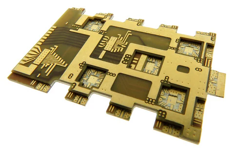
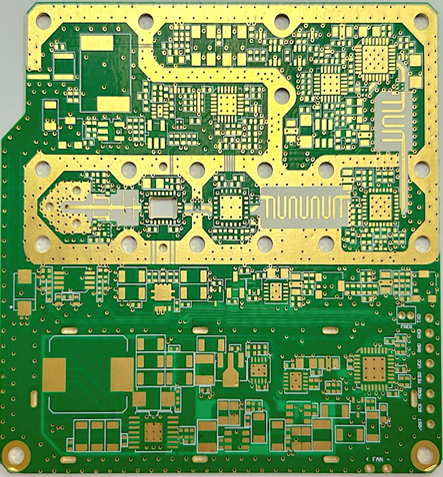
An RF Trace PCB is a printed circuit board specifically engineered to support stable radio frequency (RF) signal transmission. Unlike standard PCB traces used for low-speed digital signals, RF traces must function as controlled transmission lines, maintaining consistent impedance and minimizing signal loss.
At high frequencies, even small variations in trace width, spacing, copper roughness, or dielectric thickness can significantly affect signal performance. Therefore, RF trace PCB design requires precise engineering and manufacturing control.
Understanding RF Trace as a Transmission Line
In RF applications, PCB traces behave as transmission lines rather than simple conductors. Common RF trace structures include:
-
Microstrip
-
Stripline
-
Coplanar Waveguide (CPWG)
-
Grounded Coplanar structures
Each structure provides different field distribution characteristics and impedance control strategies. The correct selection depends on frequency range, isolation requirements, and layout constraints.
Critical Design Parameters for RF Trace PCB
1. Controlled Impedance Accuracy
Most RF systems require precise impedance values such as:
-
50Ω single-ended
-
75Ω video applications
-
100Ω differential
Impedance is influenced by:
-
Trace width
-
Dielectric constant (Dk)
-
Substrate thickness
-
Ground plane distance
Tight manufacturing tolerance ensures minimal signal reflection and stable return loss performance.
2. Minimizing Insertion Loss
As frequency increases, conductor loss and dielectric loss become more significant. RF trace PCB design must consider:
-
Low loss laminate materials
-
Smooth copper surfaces
-
Short signal path routing
-
Avoidance of unnecessary vias
Insertion loss control is especially important in GHz-range applications.
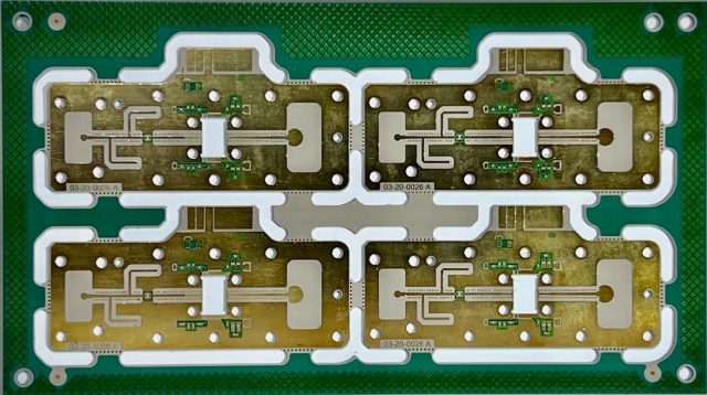
3. Via and Transition Management
Improper via design can introduce:
-
Impedance discontinuity
-
Signal reflection
-
Increased parasitic inductance
RF PCBs may incorporate:
-
Back drilling
-
Via stub reduction
-
Ground via stitching
-
Optimized layer transitions
Careful transition design maintains signal continuity.
4. Grounding and Shielding
Ground structure directly affects RF performance. Proper RF trace PCB layout includes:
-
Continuous reference planes
-
Via fences along RF traces
-
Isolation from noisy digital circuits
-
Controlled return current paths
Ground integrity improves EMI performance and signal stability.
5. Trace Length Matching and Phase Control
In RF front-end and phased array systems, phase consistency is critical. Designers must control:
-
Trace length tolerance
-
Electrical length matching
-
Symmetry in differential routing
Even millimeter-level differences can affect high-frequency signal behavior.
Applications of RF Trace PCB
RF trace PCBs are widely used in:
-
5G communication modules
-
Antenna systems
-
Radar sensors (24GHz / 77GHz)
-
Satellite communication equipment
-
IoT wireless modules
-
RF test boards
-
GPS systems
As wireless technology advances, precise RF trace engineering becomes increasingly important.
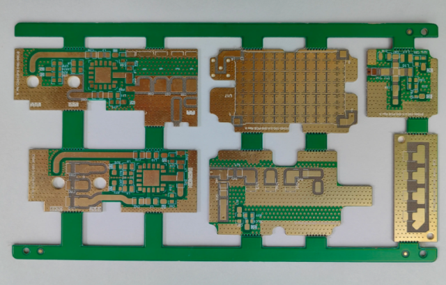
Manufacturing Capabilities for RF Trace PCB
Professional RF PCB fabrication may include:
-
Tight impedance tolerance verification
-
Controlled dielectric thickness
-
Low loss high-frequency materials
-
Precision etching for fine RF lines
-
X-ray inspection
-
Surface finish optimization (ENIG / Immersion Silver)
Consistent process control ensures repeatable RF performance across production batches.
Conclusion
RF Trace PCB design is fundamentally about precision. At high frequencies, trace geometry, material selection, grounding strategy, and manufacturing accuracy collectively determine system performance.
By combining controlled impedance routing, low loss materials, and optimized transition design, RF trace PCBs enable stable and efficient signal transmission in advanced wireless and microwave applications.
