Engineering Challenges Behind High Density PCB
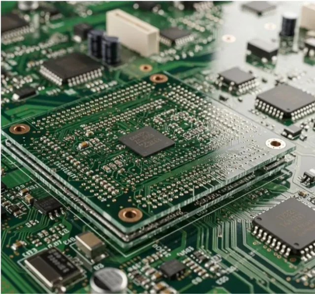
As electronic systems become more compact and functionally integrated, PCB designers are facing increasing layout complexity. A High Density PCB is not simply about placing more components on a board — it requires precise coordination between electrical design, stack-up engineering, manufacturability, and long-term reliability.
High density PCB development focuses on maximizing routing efficiency while maintaining signal integrity, thermal stability, and mechanical strength.
Core Design Challenges
1. Limited Routing Space
High pin-count processors, FPGA devices, and advanced SoCs demand dense escape routing. Designers must manage:
-
Narrow trace widths
-
Reduced spacing
-
Complex fan-out patterns
-
Multi-layer signal transitions
Efficient layer planning becomes critical at the early design stage.
2. Signal Integrity in Dense Layouts
As routing density increases, signal interaction becomes more sensitive. High density designs must address:
-
Crosstalk between adjacent traces
-
Reference plane continuity
-
Controlled impedance accuracy
-
Return path optimization
High-speed digital and RF systems are especially sensitive to layout structure.
3. Power Distribution Stability
Compact designs often combine high-speed logic with high-current power sections. A high density PCB must ensure:
-
Low impedance power delivery networks (PDN)
-
Proper decoupling strategy
-
Stable grounding architecture
-
Reduced switching noise
Power integrity directly impacts system reliability.
4. Thermal Management Within Compact Structures
Higher component density increases localized heat concentration. Effective solutions include:
-
Thermal via arrays
-
Copper balancing
-
Heavy copper planes where required
-
Optimized airflow planning
Thermal considerations must be integrated during layout rather than added afterward.
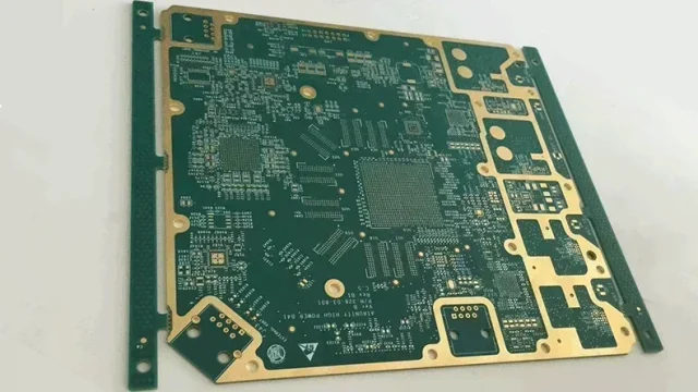
Structural Solutions in High Density PCB
To overcome design constraints, high density PCBs may incorporate:
-
High layer count stack-ups (10–24+ layers)
-
Microvia and stacked via structures
-
Blind and buried vias
-
Via-in-pad plating
-
Sequential lamination processes
-
Fine line etching technology
These technologies enable efficient routing without compromising performance.
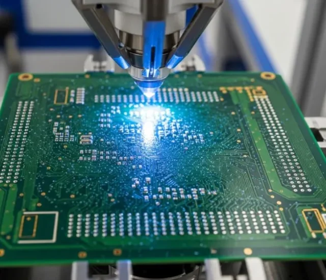
Manufacturing Considerations
High density PCB fabrication demands strict process control:
-
Tight trace width tolerance
-
Precise layer-to-layer alignment
-
Controlled dielectric thickness
-
Stable lamination cycles
-
Advanced inspection (AOI and X-ray)
Even minor deviations can impact yield in dense structures.
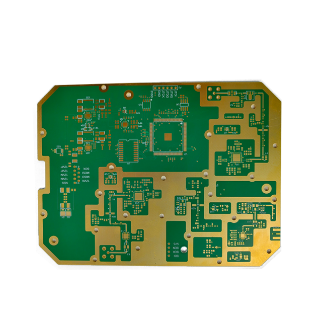
Applications Requiring High Density PCB
High density PCB technology is widely applied in:
-
AI computing modules
-
High-performance servers
-
5G communication systems
-
Automotive ADAS control units
-
Industrial robotics controllers
-
Semiconductor test boards
-
Advanced medical equipment
As system complexity increases, density optimization becomes a core design strategy.
Conclusion
High Density PCB design represents a balance between electrical performance, mechanical precision, and manufacturability. By integrating advanced routing techniques, multilayer stack-up optimization, and strict fabrication control, high density PCBs enable compact yet powerful electronic systems.
In modern electronics development, high density PCB engineering is not optional — it is foundational.
