Microvia PCB for High Density Interconnect (HDI) Design
As electronic products continue to shrink in size while increasing in functionality, traditional through-hole PCB structures are no longer sufficient. Microvia PCB technology enables higher routing density, improved signal integrity, and compact multilayer stackups, making it essential for modern high-performance electronics.
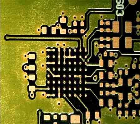
Microvias are laser-drilled vias typically with diameters ≤150μm, commonly used as blind vias or buried vias to interconnect adjacent layers in HDI PCB designs. Compared with mechanical drilling, microvia technology significantly enhances routing efficiency and reduces layer count in complex systems.
Key Features of Microvia PCB
1. Laser Drilled Microvias
High precision laser drilling ensures accurate via placement and consistent via diameter, enabling fine pitch BGA and high pin count component assembly.
2. Blind and Buried Via Structures
Supports:
-
Blind vias (outer layer to inner layer)
-
Buried vias (inner layer to inner layer)
-
Stacked microvias
-
Staggered microvias
These structures improve routing flexibility and increase wiring density.
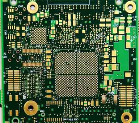
3. High Density Interconnect (HDI)
Ideal for:
-
Fine pitch IC packages
-
High pin count devices
-
Compact electronic modules
-
Miniaturized communication boards
4. Improved Signal Integrity
Shorter via stubs and reduced parasitic inductance help maintain signal integrity in high speed and RF applications.
5. Multilayer Capability
Microvia PCBs can be designed with:
-
4–20+ layers
-
Controlled impedance
-
Low loss materials
-
Sequential lamination processes
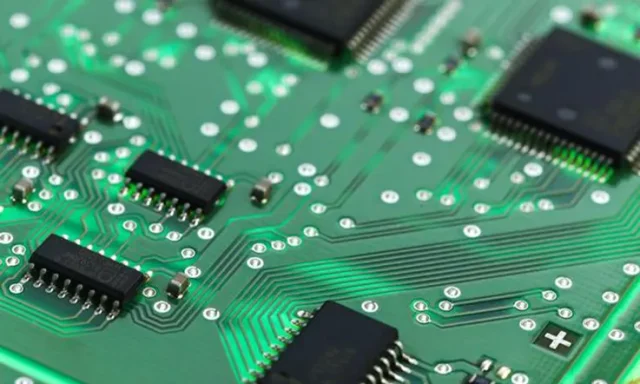
Applications of Microvia PCB
Microvia PCB technology is widely used in advanced electronic industries, including:
-
Semiconductor test boards (ATE, load board, probe card interface)
-
5G communication modules
-
RF and microwave PCBs
-
IoT devices
-
Automotive electronics
-
Medical equipment
-
Industrial control systems
-
High speed computing and networking devices
For semiconductor and IC testing applications, microvia PCBs enable high pin density routing required for modern package types such as BGA, QFN, and CSP.
Why Choose Microvia PCB for Advanced Designs
Modern electronics demand:
-
Smaller footprint
-
Higher functionality
-
Faster signal transmission
-
Greater reliability
Microvia PCB technology addresses these challenges by allowing designers to reduce layer count while maintaining performance. It also supports advanced materials such as high TG laminates and low loss substrates for high frequency environments.
When combined with controlled impedance design and precise fabrication control, microvia PCBs provide stable electrical performance for high speed digital and RF applications.
Manufacturing Considerations
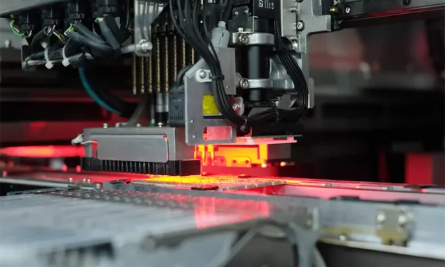
To ensure reliability, microvia PCB manufacturing requires:
-
Precise laser drilling
-
Strict via aspect ratio control
-
Sequential lamination process management
-
Reliable copper filling for stacked vias
-
Thermal stress testing and quality inspection
Proper process control ensures excellent interconnection reliability and long-term performance, especially in automotive, aerospace, and semiconductor testing environments.
Conclusion
Microvia PCB technology is a critical enabler for next-generation electronic products. Whether used in HDI designs, high speed communication boards, or semiconductor test systems, microvia structures provide enhanced routing density, improved signal integrity, and compact form factors.
As devices continue to evolve toward higher performance and miniaturization, microvia PCB solutions will remain essential for achieving advanced design goals.
