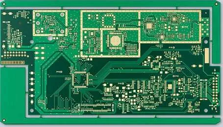
What Is a Multilayer PCB?
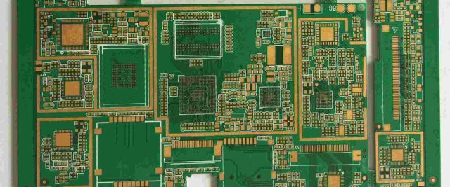
A Multilayer PCB is a printed circuit board composed of three or more conductive copper layers laminated together with insulating dielectric materials. Compared to single-sided or double-sided boards, Multilayer PCB technology allows significantly higher circuit density and more complex routing structures.
Modern electronic systems increasingly require compact size, high speed signal transmission, and high integration. Multilayer PCB design enables engineers to meet these demands while maintaining stable electrical performance.
Typical multilayer configurations include:
-
4-layer PCB
-
6-layer PCB
-
8-layer PCB
-
10+ layer PCB
-
High layer count PCB (20+ layers)
Key Features of Multilayer PCB
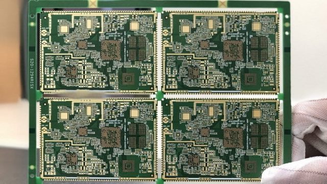
1. Higher Circuit Density
Multilayer PCB provides multiple routing layers, allowing:
-
Dense component placement
-
Complex signal routing
-
Reduced board size
-
Improved layout flexibility
This makes it ideal for compact and high-performance devices.
2. Improved Signal Integrity
With dedicated signal, power, and ground planes, Multilayer PCB helps:
-
Reduce electromagnetic interference (EMI)
-
Improve return path control
-
Maintain controlled impedance
-
Minimize signal reflection and crosstalk
These advantages are essential for high-speed digital and RF applications.
3. Better Power Distribution
Multilayer PCB structures allow internal power and ground planes, which:
-
Provide stable voltage distribution
-
Reduce noise
-
Improve thermal performance
-
Enhance overall reliability
This is particularly important for high current and high-speed systems.
4. Compact and Lightweight Design
By stacking multiple layers vertically, designers can reduce the overall PCB size while increasing functionality. This is critical in:
-
Consumer electronics
-
IoT devices
-
Communication modules
-
Portable industrial equipment
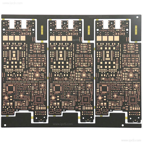
Manufacturing Capabilities
Professional Multilayer PCB fabrication includes:
-
Precision lamination processes
-
Sequential lamination for HDI structures
-
Blind and buried vias
-
Microvia drilling
-
Controlled impedance processing
-
High TG and low loss materials
-
Advanced surface finishes (ENIG, ENEPIG, immersion silver)
Strict quality control ensures accurate layer alignment, stable dielectric thickness, and consistent impedance performance.
Applications of Multilayer PCB
Multilayer PCB is widely used in:
-
5G communication systems
-
RF and microwave equipment
-
Semiconductor test boards
-
Automotive electronics
-
Industrial control systems
-
Medical devices
-
Aerospace electronics
-
Data center and server boards
As electronics become more complex and compact, multilayer designs are increasingly essential.
Advantages of Multilayer PCB
-
Higher functional integration
-
Reduced PCB footprint
-
Better electrical performance
-
Enhanced EMI shielding
-
Stable impedance control
-
Improved mechanical strength
-
Support for high layer count designs
Multilayer PCB technology provides the foundation for advanced electronic systems requiring high reliability and high-speed performance.
Conclusion
Multilayer PCB is a critical solution for modern electronics that demand high density, high speed, and high reliability. Through advanced lamination technology, precision fabrication, and strict impedance control, multilayer boards ensure consistent electrical performance across complex applications.
Selecting an experienced PCB manufacturer ensures stable quality, tight tolerances, and dependable production for your multilayer PCB projects.
