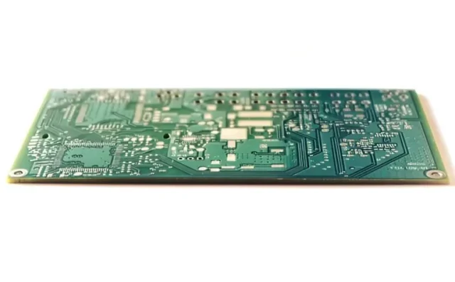
What Is a Multilayer PCB?
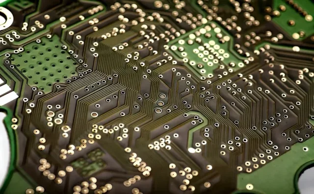
A multilayer PCB is a printed circuit board composed of multiple copper layers separated by prepreg and core materials. Unlike single-sided or double-sided PCBs, multilayer boards provide additional routing layers, allowing engineers to design high-density circuits with improved electrical performance.
Typical multilayer PCB configurations include:
-
4-layer PCB
-
6-layer PCB
-
8-layer PCB
-
10-layer and above for advanced applications
The number of layers depends on signal complexity, power distribution requirements, EMI control, and impedance control design.
Key Advantages of Multilayer PCB
1. High Circuit Density
Multilayer PCBs allow complex routing in limited board space, making them ideal for compact electronic devices such as smartphones, tablets, and IoT products.
2. Improved Signal Integrity
By incorporating dedicated ground and power planes, multilayer PCB design enhances signal integrity, reduces noise, and minimizes electromagnetic interference (EMI).
3. Controlled Impedance Capability
Advanced multilayer PCB stackups enable precise impedance control for high-speed digital PCB and RF PCB applications, ensuring reliable signal transmission.
4. Better Thermal Management
With optimized copper distribution and internal plane layers, multilayer PCBs can dissipate heat more effectively in high-power electronics.
5. Enhanced Mechanical Strength
The laminated structure increases board rigidity and durability, which is especially important in automotive and industrial environments.
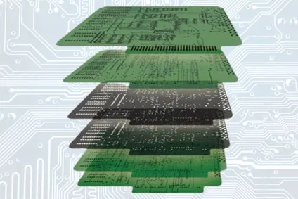
Multilayer PCB Stackup Design Considerations
Proper multilayer PCB stackup design is critical for performance and manufacturability. Key factors include:
-
Layer arrangement and symmetry to prevent warpage
-
Dielectric material selection for electrical stability
-
Copper thickness control for current-carrying capacity
-
Via structure design, including through-hole, blind, and buried vias
-
Impedance control requirements for high-speed circuits
Collaborating closely with the PCB manufacturer during the stackup planning stage ensures optimized electrical performance and cost efficiency.
Applications of Multilayer PCB
Multilayer PCBs are essential in advanced electronic systems, including:
-
Telecommunication equipment (5G base stations, routers, servers)
-
Automotive electronics (ADAS, EV control systems, infotainment)
-
Medical devices (imaging systems, monitoring equipment)
-
Industrial automation (PLC systems, robotics)
-
Consumer electronics (smartphones, laptops, wearable devices)
In high-frequency and high-speed applications, multilayer PCB design plays a vital role in maintaining signal integrity and system reliability.
Manufacturing Process of Multilayer PCB
The multilayer PCB manufacturing process involves:
-
Inner layer circuit imaging and etching
-
Layer alignment and lamination under heat and pressure
-
Drilling and via metallization
-
Outer layer patterning
-
Surface finish application (ENIG, HASL, OSP, etc.)
-
Electrical testing and quality inspection
Precision during lamination and drilling is essential to ensure layer alignment accuracy and impedance consistency.
Conclusion
A multilayer PCB is the backbone of modern electronic systems. By enabling high-density routing, controlled impedance, enhanced signal integrity, and compact design, multilayer PCBs support the rapid advancement of high-speed digital and high-frequency technologies. Whether for telecommunications, automotive, medical, or consumer electronics, multilayer PCB solutions remain critical for next-generation innovation.
