High Frequency IoT PCB Prototype: Key Materials, Design Challenges, and Manufacturing Solutions
With the rapid development of smart cities, industrial automation, and connected devices, IoT technology continues to evolve toward higher transmission speeds and wider communication bandwidths. High frequency IoT PCB prototypes play a crucial role in enabling stable wireless communication for applications such as 5G modules, smart sensors, wearable devices, and industrial IoT gateways.
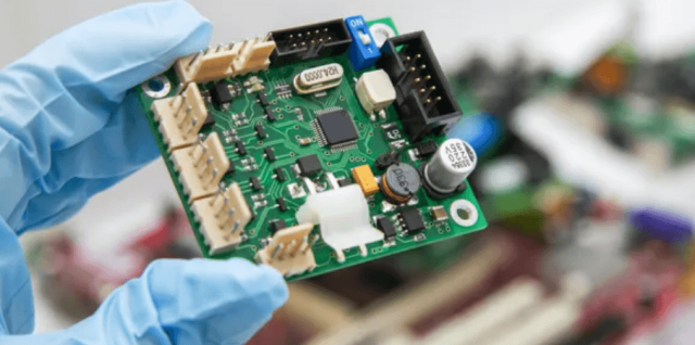
Designing and manufacturing high frequency IoT PCBs requires specialized materials, advanced layout techniques, and strict process control to ensure signal integrity and low transmission loss.
The Importance of High Frequency PCB in IoT Devices

IoT devices increasingly rely on high-frequency signals, typically ranging from hundreds of MHz to millimeter-wave frequencies. These high-speed signals are sensitive to signal attenuation, electromagnetic interference, and impedance mismatches. Therefore, high frequency PCBs are essential to maintain reliable wireless connectivity and optimize device performance.
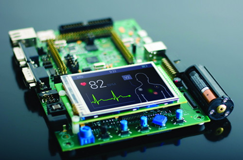
High frequency IoT PCB prototypes are commonly used in:
-
Wireless sensor networks
-
5G communication modules
-
Smart home and wearable devices
-
Industrial monitoring systems
-
Automotive radar and telematics
-
Satellite and GPS communication devices
Material Selection for High Frequency IoT PCB Prototype
Selecting the right substrate material is critical to minimizing signal loss and ensuring stable electrical performance. Compared with standard FR4, high frequency PCBs require materials with low dielectric constant (Dk) and low dissipation factor (Df).
Common materials include:
Rogers Series Materials
Rogers laminates such as RO4003C, RO4350B, and RT/duroid 5880 provide excellent electrical stability, low signal loss, and strong thermal reliability, making them ideal for RF and microwave IoT applications.
Taconic Materials
Taconic RF-35 and TLY-5 are widely used in high frequency and mmWave IoT modules due to their low loss characteristics and consistent dielectric properties.
PTFE-Based Laminates
PTFE materials are commonly used in ultra-high-frequency applications where signal integrity and thermal stability are critical.
Design Challenges in High Frequency IoT PCB Prototyping
Controlled Impedance Design
High frequency signals require precise impedance control to prevent reflection and signal distortion. PCB stack-up design, trace width calculation, and dielectric thickness must be carefully optimized.
Signal Integrity and Crosstalk Control
High-speed signals are highly sensitive to interference. Designers must optimize routing, grounding strategies, and shielding techniques to minimize noise and electromagnetic coupling.
Thermal Management
IoT modules operating at high frequency often generate significant heat. Proper thermal vias, copper balancing, and material selection help maintain long-term reliability.
Miniaturization Requirements
Many IoT devices require compact layouts, which increases routing density and demands advanced PCB manufacturing technologies such as microvias and HDI structures.
Manufacturing Considerations for High Frequency IoT PCB Prototype
Producing high frequency IoT PCBs requires specialized fabrication capabilities, including:
-
Precision impedance control testing
-
Advanced lamination processes
-
Laser drilling for microvias
-
High accuracy registration and etching
-
Strict dielectric thickness control
-
RF performance verification
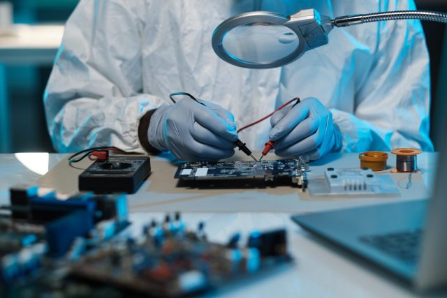
Prototype manufacturing also plays a critical role in verifying signal performance before mass production. Fast-turn prototype services help engineers evaluate design feasibility and optimize product performance.
Advantages of Professional High Frequency PCB Prototype Services
Working with an experienced PCB manufacturer ensures:
-
Stable electrical performance
-
Reliable RF signal transmission
-
Material expertise and engineering support
-
Rapid prototyping and design optimization
-
High production consistency
These advantages significantly reduce product development cycles and improve time-to-market for IoT devices.
Conclusion
High frequency IoT PCB prototypes are essential for modern wireless communication and smart device innovation. By selecting low-loss materials, optimizing RF layout design, and partnering with experienced manufacturers, companies can achieve reliable performance and long-term product stability.
As IoT technologies continue expanding into 5G, satellite communication, and industrial automation, high frequency PCB solutions will remain a key foundation for next-generation connected devices.
