A PTFE PCB is a critical technology platform for RF, microwave, and high-frequency electronic systems where low signal loss, phase stability, and dielectric consistency are non-negotiable. Compared with conventional FR-4 materials, PTFE PCB laminates offer significantly lower dielectric constant (Dk) and dissipation factor (Df), enabling superior signal integrity at GHz and mmWave frequencies.
In modern communication, aerospace, radar, and satellite applications, PTFE PCB design is often the limiting factor that determines system bandwidth, insertion loss, and long-term performance stability.
Electrical Advantages of PTFE PCB Materials
The primary advantage of a PTFE PCB lies in its ultra-low dissipation factor, which directly reduces dielectric loss in high-frequency transmission lines. This characteristic is essential for applications operating above several gigahertz, where conductor loss and dielectric loss dominate total insertion loss.
Key electrical benefits of PTFE PCB materials include:
-
Low and stable dielectric constant across wide frequency ranges
-
Extremely low dissipation factor for reduced signal attenuation
-
Improved phase consistency and reduced dispersion
-
Enhanced impedance control accuracy for RF and microwave routing
These properties make PTFE PCB laminates ideal for antennas, RF front-end modules, power amplifiers, and high-speed backplanes.
Signal Integrity and Controlled Impedance Performance
In high-frequency PCB design, impedance variation caused by dielectric inconsistency can severely degrade signal integrity. A PTFE PCB provides tighter impedance control due to its predictable dielectric behavior and minimal frequency-dependent variation.
For controlled impedance PCB designs, PTFE materials help:
-
Maintain consistent trace impedance across layers
-
Reduce impedance drift over temperature and frequency
-
Minimize reflection and return loss in RF signal paths
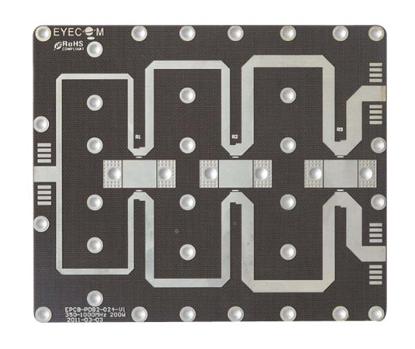
This makes PTFE PCB structures especially valuable in microwave transmission lines, microstrip, stripline, and coplanar waveguide configurations.
Thermal and Mechanical Considerations in PTFE PCB Design
Despite its electrical advantages, PTFE PCB fabrication presents unique mechanical and thermal challenges. PTFE materials typically exhibit higher coefficients of thermal expansion (CTE) compared to FR-4, requiring careful stackup symmetry and copper balancing to maintain mechanical stability.
Engineering considerations for PTFE PCB design include:
-
Managing thermal expansion to protect plated through holes
-
Ensuring lamination stability during multilayer bonding
-
Selecting appropriate reinforcement fillers for mechanical strength
-
Controlling board flatness for RF assembly reliability
A well-engineered PTFE PCB balances electrical performance with mechanical robustness.
Manufacturing Challenges and Process Control
PTFE PCB fabrication requires specialized manufacturing processes due to the material’s softness and chemical resistance. Standard FR-4 PCB processes are often insufficient.
Critical PTFE PCB manufacturing controls include:
-
Specialized drilling parameters to prevent hole deformation
-
Plasma or chemical surface treatment to ensure copper adhesion
-
Tight control of etching processes for fine RF trace geometry
-
Precision lamination techniques for multilayer PTFE PCB stackups
Consistent process control is essential to ensure repeatable electrical performance across production lots.
Applications of PTFE PCB Technology
PTFE PCBs are widely used in applications where high-frequency performance defines system success, including:
-
RF and microwave communication systems
-
Satellite and aerospace electronics
-
Radar and electronic warfare platforms
-
5G and mmWave RF modules
-
High-speed test and measurement equipment
In these systems, PTFE PCB technology enables higher bandwidth, lower loss, and more predictable signal behavior.
Engineering Perspective
A PTFE PCB is not simply a material upgrade—it is a system-level engineering choice that impacts signal integrity, thermal behavior, and manufacturing complexity. Successful PTFE PCB implementation requires close alignment between design intent, material selection, and fabrication capability.
By applying controlled impedance stackups, disciplined manufacturing processes, and RF-focused design practices, KKPCB supports engineers in delivering reliable, high-performance PTFE PCB solutions for demanding high-frequency applications.
