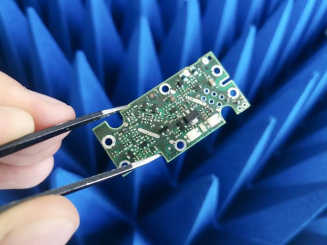
As wireless technologies continue to evolve toward higher frequencies and greater bandwidth, RF performance requirements have become more demanding than ever. From 5G communication and WiFi 6/6E to GPS, radar, and microwave RF modules, the quality of RF routing on the PCB directly impacts signal stability, insertion loss, and overall system reliability.
An RF Trace PCB is specifically engineered to support high-frequency signal transmission through optimized trace geometry, controlled impedance routing, and reliable grounding structures. Unlike ordinary digital traces, RF traces behave as transmission lines, meaning every detail—material selection, stack-up, trace width, dielectric thickness, copper roughness, and via transitions—can significantly influence RF performance.
This article explains what an RF Trace PCB is, why RF trace design matters, and how manufacturers ensure consistent performance in RF PCB fabrication.
What Is an RF Trace PCB?
An RF Trace PCB is a printed circuit board designed to route radio frequency (RF) signals and high-frequency analog signals with minimal distortion, loss, and interference. In an RF Trace PCB, traces are not simply “wires”—they are carefully designed RF transmission lines that must maintain a target impedance and stable electromagnetic behavior.
A high-quality RF Trace PCB typically includes:
-
Controlled impedance traces (commonly 50Ω single-ended or 100Ω differential when needed)
-
Microstrip RF traces (outer layer routing with a reference ground plane)
-
Stripline RF traces (inner layer routing between two reference planes)
-
Continuous ground reference planes for stable return paths
-
Via stitching and ground fencing for EMI control and isolation
-
Proper spacing and layout rules to reduce coupling and crosstalk
Because RF signals are highly sensitive to impedance discontinuities, RF Trace PCB design and manufacturing must be controlled with far higher precision than standard FR-4 boards.
Why RF Trace PCB Design Matters in High-Frequency Applications
1. Controlled Impedance Is Essential for RF Trace PCB Performance
One of the most critical goals of RF Trace PCB design is controlled impedance. When impedance changes along a trace due to geometry variation or stack-up inconsistency, the signal experiences reflections. These reflections increase return loss, reduce power transfer, and degrade system performance.
RF Trace PCBs are often designed for:
-
50Ω microstrip transmission lines
-
50Ω stripline transmission lines
-
RF matching networks and tuned circuits
-
Stable impedance routing between RF ICs, filters, and antenna ports
Controlled impedance PCB fabrication ensures the RF trace width, copper thickness, and dielectric thickness are consistent and meet the target tolerance.
2. Low Insertion Loss Improves RF Range and Signal Quality
At high frequencies, signal energy is lost due to dielectric loss and conductor loss. This results in insertion loss, which reduces signal amplitude and impacts link performance. In RF communication systems, higher loss may cause reduced range, reduced sensitivity, or poor efficiency.
A properly designed RF Trace PCB helps reduce insertion loss by:
-
Selecting low-loss PCB materials (when required)
-
Optimizing RF trace routing lengths
-
Avoiding unnecessary via transitions and stubs
-
Using smooth copper and appropriate surface finish options
For high frequency RF traces, even small improvements in loss can lead to better system-level performance.
3. Stable Return Path and Grounding Reduce Noise and EMI
In RF systems, the return path is just as important as the signal trace itself. If the RF trace crosses split planes or the ground reference is interrupted, the return current must detour, causing increased inductance, noise, and radiation.
A well-designed RF Trace PCB uses:
-
Solid and continuous ground planes
-
Short and direct return paths
-
Ground vias placed near RF trace transitions
-
Isolation techniques such as ground fencing
These methods improve RF stability, reduce EMI, and help maintain consistent RF performance.
4. Crosstalk and Coupling Become More Severe at High Frequency
As frequency increases, electromagnetic coupling between traces becomes stronger. Poor spacing or incorrect routing can cause crosstalk, which introduces noise into sensitive RF signals.
RF Trace PCB layout often includes:
-
Increased spacing between RF traces and digital lines
-
Ground shielding structures
-
Isolation zones and keep-out regions
-
Proper layer assignment (microstrip vs stripline selection)
This is especially important in compact modules where RF, digital, and power circuits must coexist on the same PCB.
Common RF Trace Structures in RF Trace PCB Design
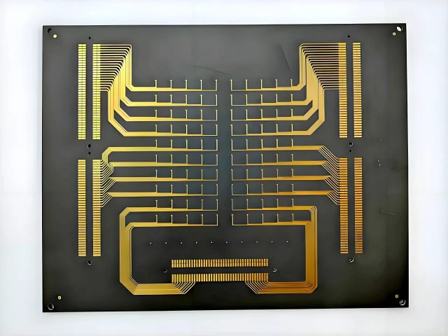
Microstrip RF Trace PCB
A microstrip is an RF trace on an outer layer, referenced to a ground plane underneath. Microstrip routing is widely used because it is easier to tune and measure, and it supports RF component placement on the same layer.
Microstrip advantages include:
-
Easier RF trace tuning and prototyping
-
Convenient RF component integration
-
Commonly used for antenna feeds and RF front-end routing
However, microstrip traces may radiate more EMI than stripline if not properly shielded.
Stripline RF Trace PCB
A stripline is an RF trace embedded between two reference planes. Stripline routing provides better shielding and lower radiation, making it suitable for noise-sensitive RF designs.
Stripline advantages include:
-
Better EMI containment
-
Improved isolation in dense designs
-
More stable impedance environment
Stripline is often used in multilayer RF Trace PCB designs where EMI control and signal integrity are critical.
RF Trace PCB Material Selection: FR-4 vs High Frequency Materials
Material selection plays a major role in RF Trace PCB performance. Standard FR-4 may be acceptable for low-to-mid frequency designs, but it can introduce higher loss at GHz frequencies.
RF Trace PCB materials may include:
-
FR-4 (for lower-frequency RF or cost-sensitive designs)
-
Rogers PCB materials for high frequency and low loss requirements
-
PTFE PCB materials for ultra-low loss microwave designs
-
Hybrid stack-ups combining RF laminate with FR-4 for cost optimization
When selecting materials for RF Trace PCB manufacturing, key parameters include:
-
Dielectric constant (Dk) stability
-
Dissipation factor (Df) for dielectric loss control
-
Thickness tolerance and consistency
-
Copper roughness effects at high frequency
A suitable material choice improves RF trace performance, reduces loss, and supports reliable controlled impedance.
RF Trace PCB Manufacturing Considerations
To ensure stable RF performance, RF Trace PCB fabrication requires precise process control and strict inspection standards.
Key manufacturing control points include:
1. Stack-Up Accuracy
RF trace impedance depends heavily on dielectric thickness and layer structure. Accurate stack-up control ensures consistent impedance and repeatable performance.
2. Trace Width and Etching Control
Small variations in trace width can cause impedance deviation. RF Trace PCB manufacturers must control etching precision and ensure consistent line geometry.
3. Controlled Impedance Testing
Controlled impedance testing verifies that RF traces meet design targets such as 50Ω or other specified impedance values. This is critical for high frequency PCB production.
4. Via Quality and Transition Design
Vias can introduce inductance and discontinuities in RF routing. High-quality RF Trace PCB fabrication focuses on:
-
Clean drilling and plating
-
Minimizing via stubs
-
Optimizing via transitions with ground vias nearby
5. Surface Finish Selection
Surface finish impacts conductor loss and solderability. Common finishes used in RF Trace PCBs include:
-
ENIG (common and reliable)
-
Immersion silver (good RF performance)
-
Other finishes based on application requirements
Selecting the right finish supports stable RF trace performance and assembly reliability.
Best Practices for RF Trace PCB Layout and Routing
To improve RF Trace PCB performance, designers commonly follow these RF routing guidelines:
-
Keep RF traces as short and direct as possible
-
Avoid sharp corners; use smooth bends or arcs
-
Maintain consistent trace width and spacing
-
Keep RF traces away from noisy digital or switching power areas
-
Place ground vias near RF transitions and connectors
-
Avoid routing RF traces across plane splits
-
Use proper RF connector footprints and launch designs
-
Ensure continuous reference planes under RF routing
These best practices help reduce reflections, minimize EMI, and improve overall high-frequency signal stability.
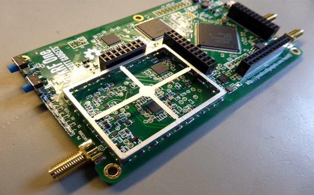
Typical Applications of RF Trace PCBs
RF Trace PCBs are widely used across industries requiring stable RF and microwave signal performance, including:
-
5G communication systems
-
WiFi modules and routers
-
GPS tracking devices
-
IoT RF communication products
-
Radar and sensing systems
-
Microwave RF amplifiers and filters
-
Antenna feed networks and RF front-end modules
-
Satellite communication and aerospace RF electronics
In these applications, RF Trace PCB design quality directly affects RF efficiency, sensitivity, and reliability.
Conclusion: Why RF Trace PCB Matters for High-Frequency Electronics
An RF Trace PCB is essential for any design where RF signals must travel with minimal loss, stable impedance, and strong resistance to EMI interference. With controlled impedance routing, optimized grounding, and precise RF trace structures such as microstrip and stripline, RF Trace PCBs provide the foundation for reliable high-frequency performance.
Whether you are designing for 5G, WiFi, GPS, radar, or microwave RF modules, selecting the right RF Trace PCB stack-up, material system, and manufacturing process is key to achieving stable results.
If you need a trusted partner for RF Trace PCB fabrication, controlled impedance testing, and high reliability production, we can support your project from stack-up review to mass production.
