A Differential Pair PCB is a printed circuit board designed to route signals in pairs of two complementary traces, where one carries the positive signal and the other carries the negative signal. Instead of relying on a single-ended reference to ground, differential signaling transmits information through the voltage difference between the two traces, making it one of the most reliable methods for high-speed, high-frequency, and low-noise PCB designs.
Differential pair PCB design is widely used in modern electronics where signal integrity, noise immunity, and EMI control are critical. As data rates continue to increase, differential pair routing has become the standard approach for high-speed interfaces and precision signal transmission.
What Is a Differential Pair PCB?
A Differential Pair PCB refers to a PCB layout where specific signal nets are routed as tightly coupled trace pairs with:
-
Equal and opposite signal polarity
-
Controlled differential impedance
-
Matched trace lengths
-
Consistent spacing and geometry
The receiver detects the voltage difference between the two traces, allowing common-mode noise to be canceled out. This makes differential pair PCB routing especially effective in electrically noisy environments and high-speed systems.
Why Differential Pair PCB Design Is Essential
As signal frequencies increase, traditional single-ended signaling becomes more susceptible to noise, crosstalk, and EMI. A differential pair PCB helps overcome these challenges by offering:
-
Superior noise immunity
-
Reduced electromagnetic interference (EMI)
-
Lower crosstalk between adjacent signals
-
Better signal integrity at high data rates
-
More stable timing performance
For modern high-speed electronics, differential pair PCB routing is no longer optional—it is a fundamental design requirement.
How Differential Pair Signaling Works on a PCB
In a differential pair PCB, the two traces carry signals that are equal in magnitude but opposite in phase. When external noise couples into both traces equally, it appears as common-mode noise, which is rejected by the differential receiver.
Key characteristics include:
-
Signal is defined by voltage difference, not absolute voltage
-
Noise cancellation improves SNR (signal-to-noise ratio)
-
Lower radiation compared to single-ended traces
-
Reduced sensitivity to ground bounce and reference noise
This principle is why differential pair PCB layouts are widely used in high-speed digital and precision analog applications.
Key Advantages of Differential Pair PCB
1. Improved Signal Integrity
Differential pair PCB routing maintains cleaner signal edges and minimizes distortion, especially at multi-Gbps data rates.
2. Excellent EMI and Noise Suppression
Closely coupled differential traces reduce electromagnetic emissions and susceptibility, making compliance with EMI regulations easier.
3. Higher Data Rate Capability
Differential signaling supports faster rise times and higher bandwidth compared to single-ended signaling.
4. Better Timing Accuracy
Matched trace lengths reduce skew, ensuring correct timing and reliable data recovery.
Common Differential Impedance Values
In a differential pair PCB, impedance control is critical. Common targets include:
-
90Ω differential impedance – USB, HDMI
-
100Ω differential impedance – Ethernet, PCIe, LVDS
-
85Ω differential impedance – Some SerDes and proprietary interfaces
Accurate impedance control depends on trace width, spacing, dielectric material, and PCB stack-up design.
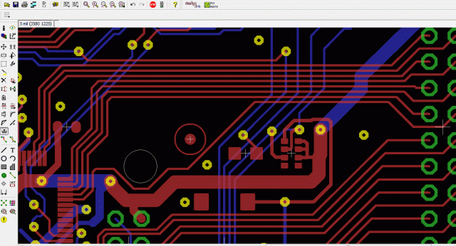
Differential Pair PCB Routing Guidelines
Proper routing is essential to achieve reliable performance:
1. Maintain Constant Spacing
Keep the spacing between the two traces consistent to ensure stable differential impedance.
2. Match Trace Lengths
Length matching minimizes skew. This is especially important for high-speed digital differential pairs.
3. Route Over Continuous Reference Planes
Avoid crossing splits or gaps in the reference plane to maintain a clean return path.
4. Minimize Layer Transitions
Each via introduces impedance discontinuities. Use fewer vias or optimize via structures when possible.
5. Control Crosstalk
Maintain adequate spacing from other signal pairs and high-speed nets.
Differential Pair PCB vs Single-Ended PCB
Compared to single-ended routing, a differential pair PCB offers:
-
Lower EMI radiation
-
Higher noise immunity
-
Better performance at high frequency
-
More predictable impedance control
While differential routing may require tighter layout rules and higher manufacturing precision, the performance benefits far outweigh the added complexity.
Typical Applications of Differential Pair PCB
Differential pair PCB design is widely used in:
-
High-speed digital interfaces (USB, HDMI, DisplayPort)
-
PCIe, SATA, and high-speed SerDes links
-
Ethernet and networking equipment
-
Telecom and data center hardware
-
High-speed backplanes and switch fabrics
-
LVDS and clock distribution systems
-
High-speed measurement and test equipment
Differential Pair PCB Material Considerations
Material selection directly impacts differential pair performance. Common choices include:
-
Standard FR-4 for moderate-speed designs
-
Low-loss PCB materials for multi-Gbps applications
-
Ultra-low-loss laminates for long channels and backplanes
Low Dk variation and low loss tangent (Df) improve impedance stability and signal quality in differential pair PCB designs.
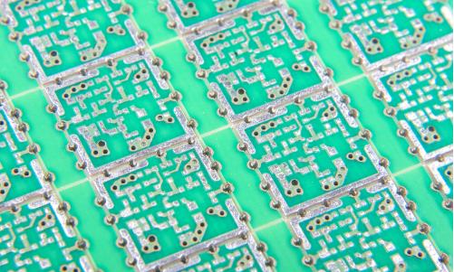
Manufacturing Considerations for Differential Pair PCB
To achieve reliable differential impedance, PCB manufacturing must control:
-
Trace width and spacing tolerance
-
Dielectric thickness accuracy
-
Copper thickness consistency
-
Layer alignment in multilayer PCBs
Impedance testing and controlled impedance fabrication are often required for high-speed differential pair PCBs.
KKPCB Differential Pair PCB Capabilities
KKPCB provides professional Differential Pair PCB manufacturing with:
-
Controlled differential impedance fabrication
-
High-speed PCB stack-up optimization support
-
Multilayer PCB capability for complex routing
-
Tight tolerance etching for trace width and spacing
-
Impedance testing and signal integrity support
-
Prototype to mass production services
Our engineering team works closely with customers to ensure differential pair PCB designs meet performance and reliability requirements.
Conclusion
A Differential Pair PCB is a cornerstone of modern high-speed and high-frequency electronic design. By leveraging differential signaling, designers can achieve superior signal integrity, reduced EMI, and reliable performance even at very high data rates. With proper routing, material selection, and controlled impedance manufacturing, differential pair PCBs deliver stable and repeatable results across a wide range of applications.
KKPCB supports high-quality Differential Pair PCB manufacturing, providing engineering expertise and production reliability from early design review to volume production.
