A High Density PCB (HDPCB) is a specialized printed circuit board designed for compact, high-performance, and high-pin-count electronic applications. HD PCBs are widely used in semiconductor test boards, IoT devices, wearable electronics, automotive systems, and high-speed communication modules, where space constraints, signal integrity, and reliability are critical.
High density PCBs combine fine-pitch component layouts, multilayer stackups, and advanced routing techniques to deliver high electrical performance in a compact form factor.
Key Features of High Density PCBs
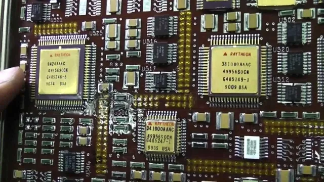
1. Fine-Pitch Component Support
HDPCBs support ICs with extremely small pitches, such as BGA, QFN, or CSP packages, enabling high pin count connections without sacrificing signal quality.
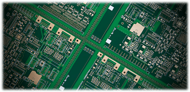
2. Advanced Multilayer Stackups
Multiple layers separate power, ground, analog, digital, and RF domains, ensuring reduced noise, crosstalk, and electromagnetic interference while maintaining high routing density.
3. Controlled Impedance and Signal Integrity
High-speed signals require precise impedance control and careful differential pair routing. HDPCBs are designed with low-loss materials, precise trace widths, and optimized via structures to maintain signal integrity.
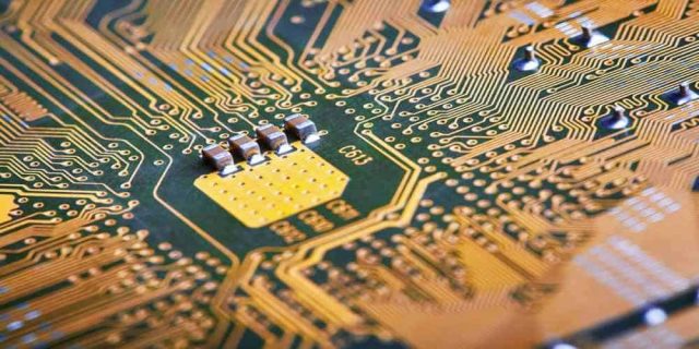
4. Microvia and Via-in-Pad Technology
Microvias, blind/buried vias, and via-in-pad designs minimize PCB real estate and improve electrical performance, enabling compact, high-density routing without compromising reliability.
5. Thermal and Power Management
High density boards integrate thermal vias, copper planes, and decoupling strategies to handle power dissipation and maintain stable operation in compact electronics.
Applications of High Density PCBs
High density PCBs are widely used in:
-
Semiconductor test boards and load boards
-
High-speed IC test platforms (5G, RF, and high-speed digital)
-
IoT and wearable device PCBs
-
Automotive electronics and ADAS IC test boards
-
Compact consumer electronics (smartphones, tablets, laptops)
HDPCBs are essential when high pin count, fine-pitch components, and signal integrity are required in limited board space.
Manufacturing Requirements for High Density PCBs
Producing high-quality HDPCBs requires:
-
Tight control of trace width, spacing, and impedance tolerances
-
Advanced multilayer lamination and registration accuracy
-
Precision drilling and via plating (microvias, blind/buried vias)
-
High-density component placement and solder mask alignment
-
Electrical testing for continuity, impedance, and signal integrity
A reliable manufacturer ensures consistent quality, high yield, and repeatable performance in high-density applications.
Conclusion
A High Density PCB is critical for compact, high-performance electronic and semiconductor test applications. Through fine-pitch component support, multilayer stackups, controlled impedance routing, and advanced microvia technology, HDPCBs deliver excellent signal integrity, reduced size, and reliable performance.
Partnering with an experienced high-density PCB manufacturer ensures high-quality, reliable boards suitable for prototype, small batch, and mass production, supporting modern electronics and semiconductor testing with precision.
