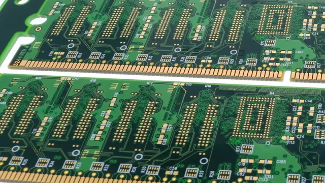
A High Density PCB is a specialized printed circuit board designed to support compact layouts, high pin count components, and complex signal routing within limited space. As electronic devices continue to shrink while increasing in performance, high density PCB technology has become essential for applications requiring high-speed data transmission, high-frequency signals, and reliable power delivery.
High density PCBs are widely used in semiconductor testing, communication systems, automotive electronics, medical devices, and industrial control, where space optimization and electrical performance are critical.
Key Features of High Density PCB Technology
1. HDI (High Density Interconnect) Structure
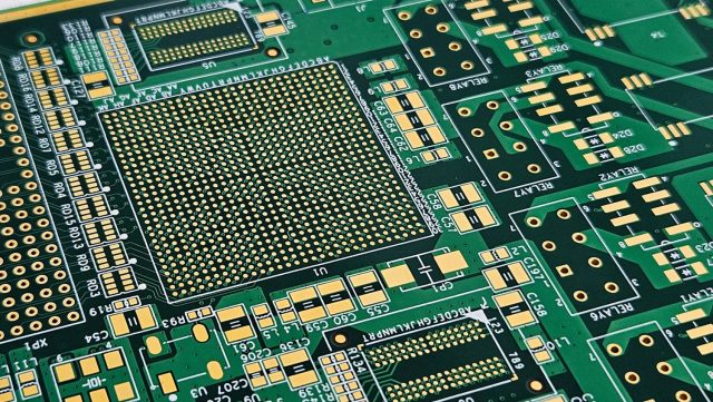
High density PCBs utilize HDI technology, including microvias, blind vias, buried vias, and sequential lamination, allowing higher routing density and improved signal integrity.
2. Fine Pitch and High Pin Count Support
Modern ICs feature fine pitch BGA and high pin count packages. High density PCBs enable reliable breakout routing using fine line/space and advanced via structures.
3. Multilayer PCB Design
High density PCBs often adopt multilayer stackups to separate signal, power, and ground layers, improving EMI control, impedance stability, and power integrity.
4. Controlled Impedance Routing
For high-speed and high-frequency designs, controlled impedance traces are essential. High density PCBs ensure precise impedance control to maintain signal integrity.
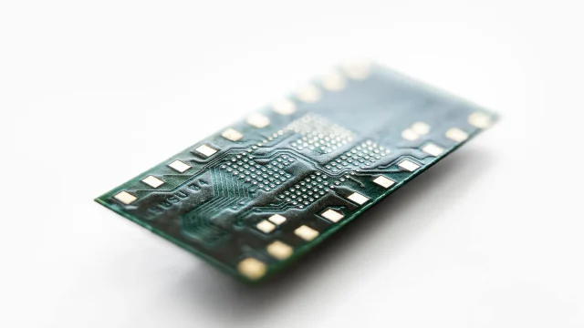
5. Compact Form Factor
By maximizing routing efficiency, high density PCBs support smaller board sizes without sacrificing electrical or mechanical reliability.
Applications of High Density PCBs
High density PCBs are widely applied in:
-
Semiconductor test PCBs (ATE, probe card, load board)
-
High-speed digital and RF communication systems
-
5G and mmWave electronics
-
Automotive ADAS and control modules
-
Medical imaging and diagnostic equipment
-
Industrial automation and embedded systems
These applications demand high reliability, precision manufacturing, and stable electrical performance.
Manufacturing Requirements for High Density PCBs
Producing high-quality high density PCBs requires:
-
Advanced HDI fabrication capability
-
Microvia drilling and sequential lamination
-
Fine line etching and registration control
-
Controlled impedance testing and verification
-
Support for prototype, small batch, and mass production
Strict process control ensures consistent quality, high yield, and long-term reliability.
Why High Density PCB Quality Matters
Poor-quality high density PCBs may lead to:
-
Signal loss, crosstalk, and impedance mismatch
-
Reduced yield and unreliable test results
-
Assembly difficulties with fine pitch components
-
Increased system failure rates
A professionally manufactured High Density PCB ensures stable signal integrity, compact design flexibility, and reliable performance in demanding electronic applications.
Conclusion
The High Density PCB is a key enabler for next-generation electronics that require compact size, high performance, and complex functionality. Through HDI technology, fine pitch routing, multilayer design, and controlled impedance, high density PCBs deliver reliable, high-quality solutions for advanced electronic systems.
Choosing an experienced high density PCB manufacturer helps accelerate product development, improve yield, and ensure long-term product reliability.
