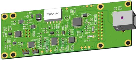
A Mixed Signal IC Test PCB is a specialized semiconductor test PCB designed to support devices that integrate analog, digital, and sometimes RF circuits on a single chip. Common mixed-signal ICs include ADCs, DACs, power management ICs (PMICs), sensors, and communication interfaces. These devices demand highly precise test environments, making mixed signal IC test PCB design and manufacturing significantly more complex than purely digital test boards.
In Automated Test Equipment (ATE) systems, the mixed signal IC test PCB serves as the critical interface between the device under test (DUT) and measurement instrumentation, ensuring accurate signal transmission, low noise coupling, and reliable power delivery.
Key Design Challenges of Mixed Signal IC Test PCBs
1. Analog and Digital Signal Isolation
Mixed-signal devices are extremely sensitive to noise. A high-quality mixed signal IC test PCB must isolate analog and digital domains through careful floorplanning, dedicated ground regions, and optimized return paths.
2. Controlled Impedance and Signal Integrity
High-speed digital and RF signals require precise controlled impedance routing, while analog signals demand clean, low-noise paths. Proper stackup design balances both requirements.
3. Power Integrity and Noise Suppression
Multiple voltage domains are common in mixed-signal ICs. Robust power distribution networks (PDN), decoupling strategies, and low-inductance vias are essential to maintain stable operation.
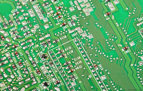
4. High-Density and High Pin Count Routing
Modern mixed-signal ICs often feature fine-pitch packages and high I/O counts. HDI PCB technology enables efficient fan-out while preserving signal integrity.
5. Mechanical Precision and Test Socket Alignment
Accurate socket alignment and mechanical stability ensure repeatable electrical contact across thousands of test cycles.
Applications of Mixed Signal IC Test PCBs
Mixed signal IC test PCBs are widely used in:
-
ADC and DAC testing
-
Power management IC (PMIC) validation
-
Sensor and interface IC testing
-
RF-enabled mixed-signal devices
-
Automotive, industrial, and IoT semiconductor testing
These applications require high accuracy, low noise, and stable performance, making professional PCB engineering essential.
Materials and Manufacturing Considerations
Producing a reliable Mixed Signal IC Test PCB requires careful material and process selection:
-
High-Tg FR-4 for standard mixed-signal applications
-
Low-loss laminates for high-speed and RF signal paths
-
Hybrid stackups combining analog and RF requirements
-
HDI and multilayer PCB fabrication (often 10–24+ layers)
-
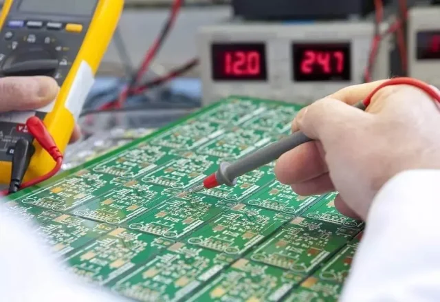
Controlled impedance measurement and verification
These factors ensure consistent performance across varied test conditions.
Why Mixed Signal IC Test PCB Quality Matters
Poorly designed mixed signal IC test PCBs can introduce noise coupling, measurement errors, and false test failures. A high-quality mixed signal IC test PCB delivers:
-
Accurate analog and digital measurement results
-
Reduced test uncertainty and debugging time
-
Improved test repeatability and yield
-
Reliable performance in high-volume production testing
Conclusion
The Mixed Signal IC Test PCB is a vital component in modern semiconductor testing environments, enabling accurate validation of complex ICs that combine analog, digital, and RF functionality. Through advanced PCB layout techniques, controlled impedance routing, robust power integrity, and precise manufacturing, mixed signal IC test PCBs ensure reliable, repeatable, and high-precision semiconductor testing.
Choosing an experienced mixed signal IC test PCB manufacturer is essential to achieving long-term testing accuracy and production success.
