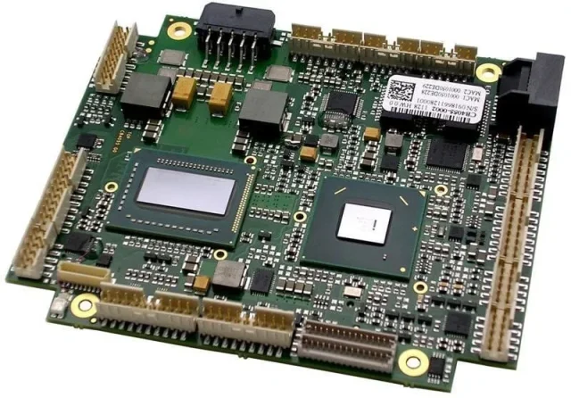
As electronic devices become smaller, faster, and more complex, traditional PCB technologies often struggle to meet space and performance requirements. The HDI PCB (High-Density Interconnect PCB) addresses these challenges by enabling ultra-dense routing, shorter signal paths, and improved electrical performance in compact form factors.
A professionally designed HDI PCB is essential for modern high-speed, high-pin-count, and miniaturized electronic systems.
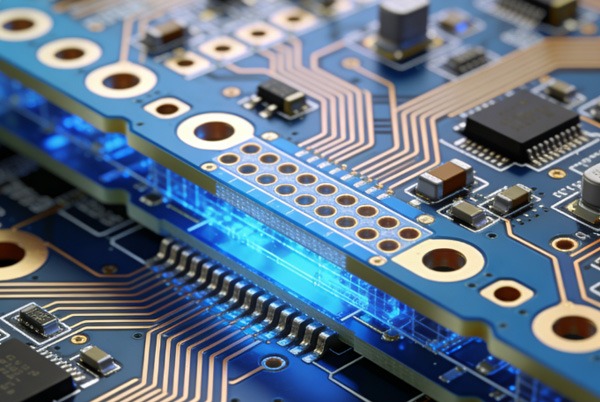
What Is an HDI PCB?
An HDI PCB is a printed circuit board that uses advanced interconnect technologies such as:
-
Microvias (laser-drilled vias)
-
Fine trace and space geometry
-
Sequential lamination
These features allow higher wiring density compared to conventional PCBs.
Why HDI PCB Technology Matters
HDI PCBs are used when:
-
Component pin counts exceed routing capability of standard PCBs
-
Board size must be minimized
-
High-speed performance demands shorter signal paths
HDI technology enables compact designs without sacrificing reliability.
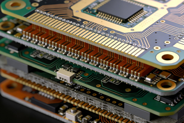
Microvia Structures and Via-in-Pad Design
Microvias are the foundation of HDI PCBs. Common structures include:
-
Stacked microvias
-
Staggered microvias
-
Via-in-pad with copper filling
These structures support efficient breakout and high-density routing.
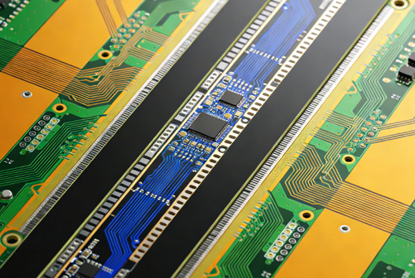
Fine-Line Routing for High-Speed Signals
HDI PCBs support ultra-fine trace and spacing, enabling:
-
Dense signal routing
-
Improved impedance control
-
Reduced signal path length
Shorter paths enhance signal integrity and reduce loss.
Signal Integrity Advantages of HDI PCBs
HDI technology improves signal integrity by:
-
Minimizing via stubs
-
Reducing parasitic capacitance and inductance
-
Improving return path continuity
These benefits are critical for high-speed digital and RF designs.
Power Integrity in HDI PCB Designs
Compact layouts increase power integrity challenges. HDI PCBs address this with:
-
Distributed decoupling placement near devices
-
Low-inductance power delivery paths
-
Optimized plane segmentation
Stable power delivery supports reliable operation.
Material and Stackup Design
HDI PCBs often use:
-
High-Tg FR-4 for mechanical stability
-
Low-loss laminates for high-speed layers
-
Symmetrical stackups for warpage control
Material selection balances performance and cost.
Manufacturing Challenges and Process Control
HDI PCB fabrication requires strict process control, including:
-
Laser drilling accuracy
-
Via filling and planarization
-
Layer-to-layer registration
Experienced manufacturers ensure high yield and reliability.
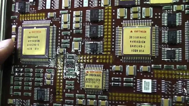
Typical Applications of HDI PCBs
HDI PCBs are widely used in:
-
Smartphones and wearable devices
-
High-speed computing and networking systems
-
Semiconductor test and evaluation boards
-
Medical and automotive electronics
These applications demand compact size and high performance.
Choosing an HDI PCB Manufacturing Partner
When selecting an HDI PCB manufacturer, consider:
-
Microvia and sequential lamination capability
-
Fine-line and via-in-pad experience
-
Controlled impedance and electrical testing support
-
Strong engineering collaboration
The right partner ensures manufacturable and reliable HDI designs.
Conclusion
The HDI PCB is a key technology enabling compact, high-speed, and high-density electronic designs. Through advanced microvia structures, fine-line routing, and precise manufacturing, HDI PCBs deliver superior electrical performance and design flexibility.
Partnering with an experienced HDI PCB supplier is essential for achieving consistent quality from prototype to mass production.
