As electronic devices continue to evolve toward higher speeds, greater bandwidth, and higher operating frequencies, impedance control on PCBs has become a critical requirement rather than an optional design consideration. In high-speed PCB, RF PCB, and high-frequency circuit design, improper impedance control can lead to signal degradation, EMI issues, and overall system instability.
This article explains why impedance control on PCBs matters, how it impacts signal integrity, and why close collaboration between design and PCB manufacturing is essential for reliable performance.
What Is Impedance Control on PCBs?
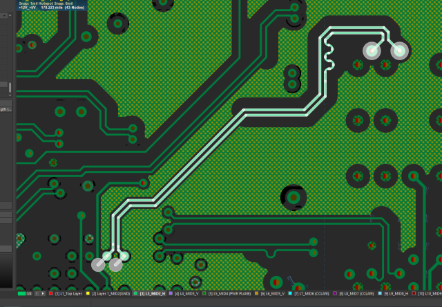
Impedance control on PCBs refers to designing and manufacturing PCB traces so that their characteristic impedance matches a specified target value, such as 50Ω, 90Ω, or 100Ω.
This impedance is determined by multiple factors, including:
- Trace width and thickness
- Dielectric constant (Dk) of PCB materials
- Dielectric thickness between signal layers and reference planes
- Copper thickness and surface finish
In high-speed and high-frequency PCB design, controlled impedance ensures predictable signal behavior throughout the transmission path.
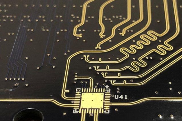
Why Impedance Control Is Critical for High-Speed PCB Design

In high-speed PCB applications, digital signals have extremely fast edge rates. When impedance is not properly controlled:
- Signal reflections occur at impedance discontinuities
- Timing skew and eye diagram degradation increase
- Crosstalk and noise margins worsen
Accurate PCB impedance control minimizes reflections and ensures clean signal transmission, which is essential for interfaces such as USB, HDMI, PCIe, and DDR memory.
Importance of Impedance Control in RF and High-Frequency Circuits
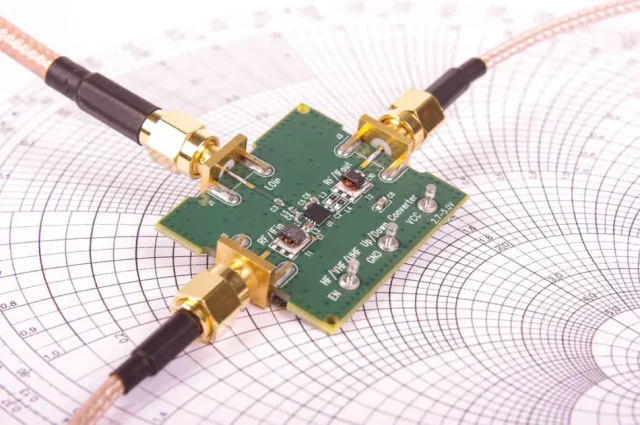
For RF PCB and high-frequency PCB designs, impedance control is even more critical.
- RF signals are highly sensitive to impedance mismatch
- Small impedance variations can cause power loss and signal distortion
- Impedance mismatch reduces antenna efficiency and system gain
Maintaining precise controlled impedance PCB structures allows RF signals to propagate with minimal loss, ensuring stable and repeatable RF performance.
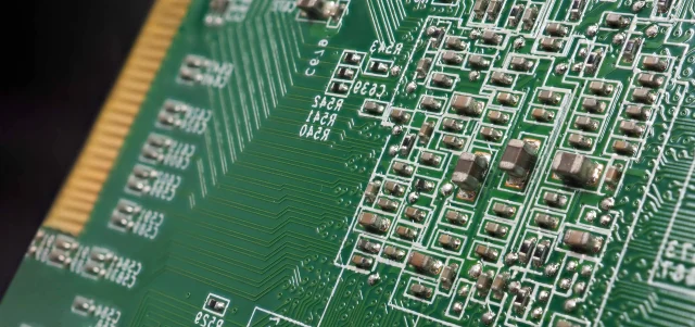
Key Manufacturing Factors Affecting PCB Impedance Control
Even with a well-designed layout, impedance control on PCBs depends heavily on manufacturing accuracy.
Key factors include:
- PCB material selection and Dk tolerance
- Dielectric thickness control during lamination
- Trace width accuracy after etching
- Copper plating thickness and uniformity
- Solder mask influence on impedance-controlled traces
A reliable PCB manufacturer must tightly control these variables to achieve consistent impedance results.
Impedance Testing and Verification
To ensure proper impedance control on PCBs, testing is essential.
- TDR (Time Domain Reflectometry) testing measures actual impedance values
- Test coupons represent real PCB stack-up conditions
- Common tolerances include ±10% or tighter ±5% for advanced designs
Impedance testing verifies that the finished PCB meets design and performance requirements.
Conclusion
Whether for high-speed PCB, RF PCB, or high-frequency circuit design, impedance control on PCBs is fundamental to achieving reliable signal integrity and stable electrical performance. Poor impedance control can compromise even the most advanced designs, while accurate impedance control enhances system reliability and product quality.
By combining precise PCB design with experienced controlled impedance PCB manufacturing, engineers can ensure optimal performance across high-speed, RF, and high-frequency applications.
