As electronic systems continue to evolve toward higher speeds, greater functionality, and reduced form factors, Buried Via PCB structures have become a critical enabler for advanced multilayer designs. By allowing interlayer connections without penetrating the outer layers, buried vias unlock higher routing density, improved signal integrity, and enhanced EMI control. However, these electrical advantages must be carefully balanced against manufacturability, cost, and yield considerations. Achieving this balance is the key to successful buried via PCB implementation.
The Role of Buried Via PCB Technology in Modern Electronics
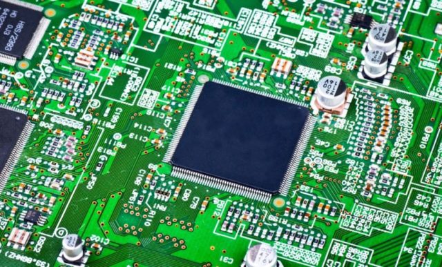
A Buried Via PCB is defined by vias that connect one or more internal layers without extending to the external surfaces of the board. Unlike through-hole vias, buried vias free up valuable surface routing space and reduce via stubs, making them particularly advantageous for high-speed digital PCB, RF PCB, and high layer count PCB applications.
From an electrical perspective, buried vias enable:
-
Shorter signal paths and reduced parasitic inductance
-
Improved impedance continuity in controlled impedance PCB designs
-
Lower crosstalk and enhanced signal integrity in dense routing environments
These benefits are especially important in applications such as data centers, industrial automation, medical electronics, and high-reliability communication systems.
Electrical Performance Considerations in Buried Via PCB Design
When designing a buried via PCB, electrical performance is often the primary motivation. However, performance gains are only realized when buried vias are correctly engineered within the overall stackup.
Key electrical factors include:
-
Impedance control: Buried vias help maintain stable impedance by minimizing via stubs and discontinuities, critical for high-speed differential pairs.
-
Signal integrity: Reduced reflection and insertion loss improve eye diagrams and timing margins in high-speed PCB designs.
-
EMI and EMC performance: Internal via transitions limit radiation paths, supporting tighter EMI compliance.
-
Power integrity: Buried vias can be optimized to reduce loop inductance between power and ground planes.
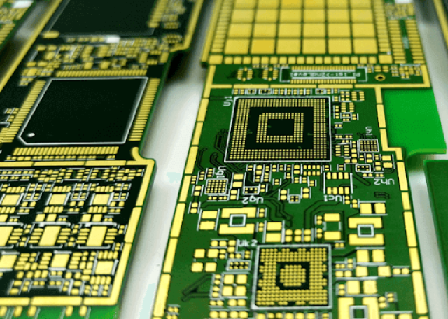
These electrical advantages make buried via PCB structures particularly valuable in high-density interconnect (HDI) and multilayer PCB architectures.
Manufacturability Challenges of Buried Via PCB Structures
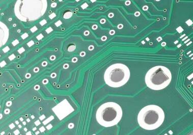
While electrically attractive, buried via PCB designs introduce additional manufacturing complexity. Each buried via layer pair requires a dedicated lamination cycle, increasing process steps and potential risks.
From a manufacturing standpoint, key challenges include:
-
Multiple lamination cycles, which increase production time and cost
-
Via registration accuracy, critical to ensure reliable interlayer connections
-
Drilling and plating yield, especially for small-diameter buried vias
-
Thermal stress accumulation, which can affect long-term reliability
Without proper DFM (Design for Manufacturability) planning, buried via PCBs can suffer from low yields, misregistration, or inconsistent plating quality.
Achieving Balance Through Stackup and Process Optimization
Balancing electrical performance and manufacturability starts with a rational stackup strategy. Not every design requires buried vias across all internal layers. Selective use of buried vias—combined with through vias or blind vias—often delivers the best compromise.
Best practices include:
-
Limiting the number of buried via layer pairs to reduce lamination complexity
-
Aligning buried via usage with critical signal layers only
-
Coordinating via aspect ratios with proven drilling and plating capabilities
-
Designing stackups that maintain symmetry to minimize warpage
Close collaboration between PCB designers and manufacturers is essential to ensure buried via PCB structures remain both electrically optimized and manufacturable at scale.
Cost, Yield, and Reliability Trade-Offs
From a commercial perspective, buried via PCB designs must justify their added cost. While they increase fabrication expense, they often reduce overall system cost by enabling smaller board sizes, higher integration, and better electrical margins.
A well-balanced buried via PCB design can achieve:
-
Higher first-pass yield through controlled process windows
-
Improved long-term reliability under thermal cycling
-
Reduced rework and field failure risk
When evaluated across the full product lifecycle, properly engineered buried via PCBs often deliver superior value despite higher upfront fabrication complexity.
Conclusion
Buried Via PCB structures represent a powerful tool for meeting the electrical demands of modern high-density and high-speed electronics. However, their success depends on striking the right balance between electrical performance and manufacturability. By integrating sound stackup design, realistic DFM constraints, and close manufacturer collaboration, engineers can fully leverage buried via PCB technology without sacrificing yield, reliability, or cost efficiency.
In advanced PCB design, the goal is not simply to push technical limits—but to push them wisely.
