A Double Layer HF PCB may appear structurally simple, yet in high-frequency engineering it provides a remarkably efficient platform for low-loss propagation, stable impedance, and predictable electromagnetic behavior. When RF designers need high-frequency stability without the cost or stackup escalation of multilayer PCBs, a Double Layer HF PCB offers the ideal balance between manufacturability and performance—especially in microwave, sub-6 GHz, and even low mmWave applications.
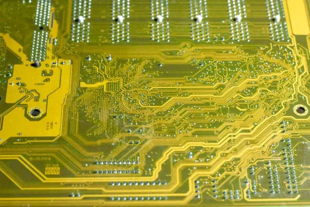
The electrical behavior of a Double Layer HF PCB is dominated by the dielectric material selection and the microstrip or coplanar transmission line design. HF materials such as Rogers, Taconic, and PTFE-based substrates reduce dielectric loss, minimize dispersion, and keep Dk/Df stable across operating temperatures. These properties are critical because high-frequency communication systems demand consistent propagation velocity and tight impedance control. When paired with optimized conductor width, surface roughness management, and precise copper thickness, a Double Layer HF PCB can deliver insertion-loss performance approaching much more complex RF stackups.
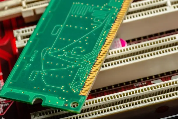
Grounding strategy is another defining advantage. The two-layer architecture creates a clean reference plane that supports microstrip HF routing with minimal mode conversion and superior phase stability. By controlling return paths, reducing ground discontinuities, and implementing via-fencing or edge-plating, a Double Layer HF PCB can suppress EMI leakage and improve high-frequency confinement. These grounding enhancements directly improve S-parameter behavior, especially S21 transmission quality and S11 return loss at higher frequencies.
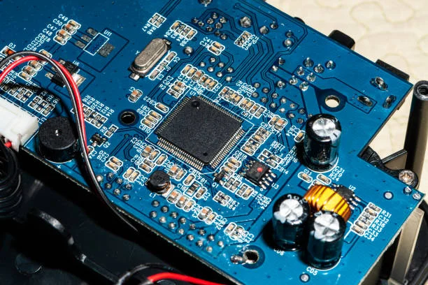
Thermal performance also benefits from the two-layer structure. Because a Double Layer HF PCB has reduced dielectric thickness and simpler heat flow paths, RF power devices, LNAs, PAs, and oscillators dissipate heat more uniformly. This thermal uniformity stabilizes Dk, prevents drift in high-frequency components, and improves the long-term reliability essential for communication modules, radar sensors, GNSS terminals, and IoT RF front-ends.
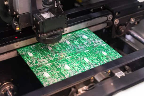
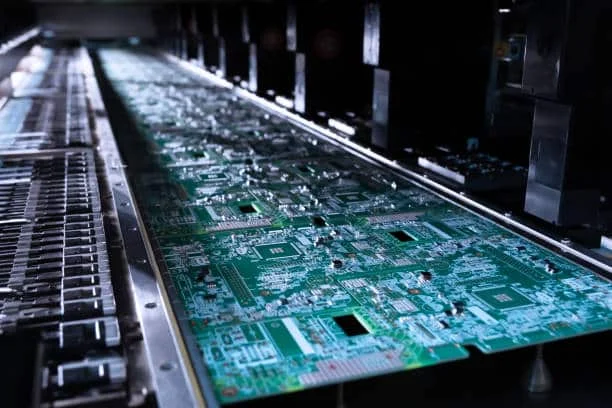
Manufacturing precision plays a decisive role. KKPCB’s high-frequency fabrication processes—controlled etching, laser-drilled micro-vias (when required), copper surface polishing, and strict dielectric thickness tolerance—ensure that every Double Layer HF PCB meets the impedance accuracy and low-loss requirements demanded by RF designers. The ability to fine-tune conductor width, copper roughness, and substrate type allows KKPCB to tailor each Double Layer HF PCB for specific system performance targets.
In modern RF engineering, the Double Layer HF PCB is no longer a basic entry-level solution. It is a highly optimized, high-frequency-ready platform capable of supporting advanced wireless communication systems, radar nodes, satellite submodules, and precision sensing devices. With careful design and materials selection, a Double Layer HF PCB provides a clean, reliable, and cost-efficient foundation for next-generation high-frequency electronics—proving that simplicity, when engineered correctly, can outperform complexity.
