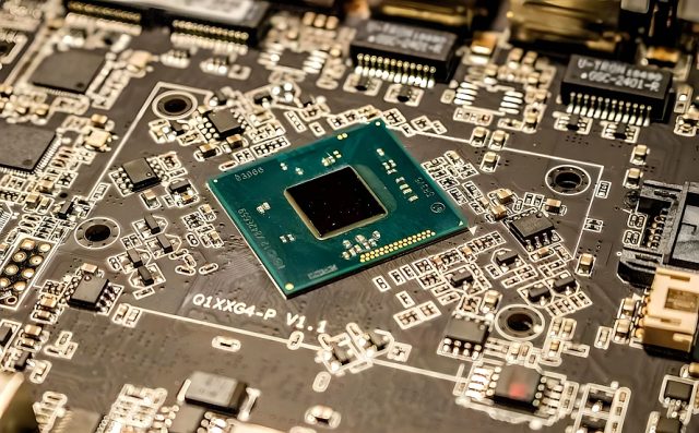
A High Speed PCB is no longer a specialty board reserved for telecom giants—it has become the core platform for every high-bandwidth, low-latency, high-frequency electronic architecture. Whether powering 56G/112G SerDes, PCIe 5.0/6.0 interconnects, next-generation routers, AI accelerator hardware, or advanced radar/5G infrastructure, the High Speed PCB defines the system’s ultimate signal integrity, timing accuracy, power efficiency, and thermal reliability.
Because modern data interfaces now push physical limits, the High Speed PCB must support tight impedance control, ultra-low insertion loss, micro-scale routing geometries, and multi-gigahertz dielectric stability. Engineering challenges that were once optional—skew balancing, reference-plane continuity, via stub suppression, return-path optimization—are now mandatory. A High Speed PCB is effectively a microwave structure, not a simple interconnect substrate.
1. Material Engineering for High Speed PCB Signal Integrity

High-speed transmission lines require PCB materials with:
-
Stable dielectric constant (Dk) across frequency and temperature
-
Ultra-low dissipation factor (Df) to minimize signal loss
-
Smooth copper profiles to reduce conductor loss at high frequencies
High-performance materials such as Megtron 6, I-Speed, Rogers RO4350B, and Taconic RF series are frequently selected for High Speed PCB stackups. These laminates allow transmission lines to maintain controlled impedance even at data rates above 112 Gbps, where traditional FR-4 fails.
The interaction between dielectric Dk/Df stability and copper roughness defines the total insertion loss for every differential pair—making material selection the most critical foundation of High Speed PCB engineering.
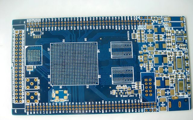
2. Precision Stackup Design: The Heart of Every High Speed PCB
A modern High Speed PCB demands a multi-layer stackup with:
-
Dedicated high-speed stripline/microstrip layers
-
Continuous reference-plane architecture
-
Balanced copper distribution for warpage control
-
Segregated analog/RF/digital power zones
Stackup design directly influences impedance uniformity, crosstalk suppression, and EMI behavior. Engineers optimize dielectric thickness, copper weight, and spacing to keep propagation delay, attenuation, and phase skew within limits. For sub-1 ps skew budgets, this becomes a mathematically precise discipline.
A well-engineered High Speed PCB stackup reduces mode conversion, minimizes odd/even-mode imbalance, and ensures predictable transmission line behavior across wide temperature and frequency ranges.
3. Advanced Routing Techniques for High Speed PCB Interconnects
As data rates climb, routing rules for a High Speed PCB tighten drastically. Critical techniques include:
-
Differential pair length and phase matching
-
Tight control of trace width/spacing for fixed impedance
-
Minimizing layer transitions to avoid stub formation
-
Back-drilling or laser-drilling vias for signal cleanliness
-
Ground-via stitching around high-speed channels
The High Speed PCB must treat every millimeter of copper as an RF path. This level of discipline prevents reflections, overshoot, jitter accumulation, and modal imbalance.
Crosstalk is another critical constraint. At multi-gigabit speeds, even small trace coupling can corrupt eye diagrams and shrink system margins. Proper isolation strategies—trace spacing, shielding vias, reference-plane segmentation—are mandatory for robust High Speed PCB performance.
4. Power Integrity & Thermal Reliability in High Speed PCB Systems
High-speed digital systems pull large transient currents during switching events. A High Speed PCB combats this through:
-
Low-inductance power delivery networks (PDN)
-
High-density decoupling schemes
-
Thin dielectric power cores
-
Distributed stitching capacitors
Thermal stability matters equally. High-frequency copper loss creates heat, and high-layer-count High Speed PCB constructions require efficient heat spreading using thermal vias, embedded copper coins, or hybrid metal-backed structures.
A thermally optimized High Speed PCB protects timing stability, improves mean time to failure (MTTF), and ensures continuous operation under harsh data-center or telecom loads.
5. Manufacturing Tolerances Define High Speed PCB Performance
Manufacturers play a decisive role in the success of High Speed PCB engineering. High-speed tolerances require:
-
Accurate impedance calibration
-
Controlled etching for consistent trace geometry
-
Low-roughness copper foil plating
-
High-precision lamination with low Z-axis expansion
-
Advanced laser via drilling for microvia reliability
Because every micron matters, a High Speed PCB must be fabricated using equipment capable of measuring and controlling extremely tight tolerances. This is where prototype accuracy and mass-production repeatability directly influence system speed and reliability.
6. Applications Requiring Cutting-Edge High Speed PCB Engineering
The rapid adoption of high-bandwidth technologies depends on High Speed PCB performance to achieve stable operation. Key application fields include:
-
5G/6G base stations and massive MIMO systems
-
High-performance computing (HPC) and AI accelerators
-
Automotive radar and ADAS processing units
-
Data-center switches and transceivers
-
Aerospace and defense communication modules
-
High-frequency instrumentation and test equipment
Every one of these environments demands uncompromising signal integrity, low jitter, low loss, and long-term reliability—hallmarks of a properly engineered High Speed PCB.
