5G mmWave hardware doesn’t leave much room for layout mistakes. When operating above 24 GHz, a few microns of misalignment, a poorly shaped via stub, or an uncontrolled dielectric transition can collapse RF integrity. That is why advanced blind via PCB layouts have become a core enabling technology for minimizing crosstalk, stabilizing impedance, and preserving low-loss propagation across dense, multilayer 5G mmWave systems.
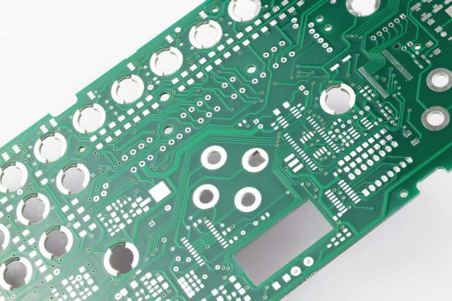
At these bands, every interconnect behaves like a resonant structure. Blind vias reduce vertical traversal distance, suppress unnecessary parasitic inductance, and cut down on multi-layer coupling that typically injects noise into sensitive RF channels.
Blind Via PCB Layouts: The mmWave Advantage
A blind via is not just a mechanical shortcut. It is an RF stabilizer. In 5G mmWave modules, they provide several critical advantages:
• They limit electromagnetic coupling paths that trigger crosstalk between high-frequency channels.
• They preserve controlled-impedance routing by minimizing the discontinuities created when signals move between layers.
• They reduce stub length, eliminating the mini-resonators that often corrupt phase linearity and S-parameter accuracy.
• They support HDI PCB architectures, enabling tighter pitch, shorter trace lengths, and cleaner RF transitions.
In dense phased-array front-ends, where beamforming accuracy depends on picosecond-level timing, blind via optimization directly improves EVM, insertion loss, and phase consistency.
Crosstalk Control in High-Density mmWave Boards
Crosstalk in mmWave boards is primarily driven by three mechanisms: near-field magnetic coupling, dielectric leakage, and parallel microstrip interactions. Advanced blind via structures counter these issues by:
• Shortening vertical interconnect paths, reducing field spread.
• Allowing signals to remain confined within designated RF layers.
• Supporting isolation-enhancing stackups using low-loss laminates such as RO4350B, RO4835, Megtron 6, or PTFE composites.
By combining blind vias with embedded ground vias, stitching fences, and low-Df dielectrics, designers achieve stable, low-noise transmission even in multi-antenna modules.
Preserving Impedance Precision at mmWave Speeds
In 5G mmWave systems, impedance tolerances often fall within ±5% or better. Blind via PCB engineering boosts this precision through:
• Controlled aspect ratios and laser-drilled via geometries.
• Smooth, copper-filled via transitions with predictable inductive behavior.
• Shorter and cleaner RF paths free from long stubs or uneven plating.
• Layer-specific impedance tuning that prevents mode-conversion and reflection.
The result is ultra-consistent impedance performance across all RF layers, which preserves:
• High-Q resonance
• Low reflection coefficients
• Minimal insertion loss
• Stable phase propagation
This is the backbone of beamforming accuracy and high-capacity 5G mmWave radio performance.
Enabling High-Power, Low-Loss 5G Modules
As mmWave modules scale toward higher channel counts and higher power levels, blind via PCBs also deliver:
• Improved thermal spreading via copper-filled microvias
• Reduced current crowding
• Lower RF heating losses
• Enhanced reliability under fast thermal cycling
These traits allow 5G mmWave equipment—CPE units, small-cells, phased-array units, repeaters—to operate with high stability even in harsh outdoor environments.
Conclusion
Advanced blind via PCB layouts are no longer optional—they are fundamental to achieving low-loss, low-noise, impedance-stable performance in modern 5G mmWave systems.
With optimized HDI structures, controlled impedance transitions, low-loss materials, and precise via engineering, designers unlock a level of RF integrity that supports higher bandwidth, stronger beamforming accuracy, and cleaner mmWave propagation.
5G mmWave hardware keeps pushing the limits of physics, and blind via PCB engineering is one of the sharpest tools available for staying ahead of those limits.
