5G communication systems rely on stringent impedance accuracy, low insertion loss, and predictable phase stability to maintain signal integrity across multi-gigabit transmission channels. At mmWave and sub-6 GHz bands, even slight deviations in controlled impedance routing can introduce reflection, jitter accumulation, and eye-diagram degradation.
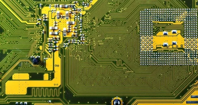
Impedance Controlled PCBs engineered for 5G must balance dielectric uniformity, copper surface roughness, high-frequency loss characteristics, and stackup stability under temperature cycling. Through precise material selection and impedance-calibrated fabrication, KKPCB delivers high-speed routing structures that preserve controlled impedance tolerance within ±5% across all layers, enabling consistent RF transmission and robust link performance for base stations, RU/DU units, massive-MIMO radios, and 5G small-cell platforms.
Core Engineering Challenges
| Challenge | Engineering Impact |
|---|---|
| Impedance drift in differential pairs | Reflection, reduced S-parameters, degraded 5G NR throughput |
| Dielectric Dk variation | Eye-diagram shrinkage, timing skew, RF mismatch |
| Copper roughness-induced loss | Increased insertion loss and degraded EVM |
| High-speed crosstalk | Inter-channel interference in dense 5G boards |
| Thermal cycling instability | Impedance shift and stackup warpage |
5G electronics—particularly mmWave radios—require the impedance controlled PCB to maintain tight tolerances under dynamic operating temperatures and modulated high-frequency workloads.
Material Science & Dielectric Performance
| Parameter | Typical Value | Engineering Benefit |
|---|---|---|
| Dielectric Constant (Dk) | 3.45–3.75 | Controlled impedance predictability across RF layers |
| Dissipation Factor (Df) | 0.002–0.004 | Reduced insertion loss at 5G high-speed lanes |
| Copper Roughness | <0.8 μm | Lower conductor loss, cleaner eye-diagrams |
| Tg | 180–200°C | Suitable for multilayer 5G stackups |
| CTE | <15 ppm/°C | Stable differential impedance under cycling |
Such material characteristics directly improve impedance uniformity, signal integrity, and high-speed routing quality.
KKPCB Case Study — 5G Sub-6 GHz Base Station
Client Requirement:
A telecom OEM needed an 8-layer impedance controlled PCB enabling clean 5G NR transmission at 3.5 GHz and 8+ Gbps digital links. ±8% impedance drift from a previous supplier caused elevated BER and link margin degradation.
KKPCB Engineering Measures:
• Implemented hybrid low-loss laminate + RCC dielectric for impedance accuracy
• Applied controlled copper roughness with reverse-treated foil
• Integrated TDR calibration traces on every panel
• Performed HFSS-driven optimization of microstrip and stripline structures
Measured Results
| Parameter | Requirement | KKPCB Result |
|---|---|---|
| Impedance Tolerance | ±8% | ±3.2% |
| Insertion Loss @10 GHz | <0.45 dB/in | 0.31 dB/in |
| Phase Deviation | <1.5° | 0.8° |
| Crosstalk (Near-End) | <-30 dB | -36 dB |
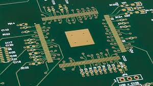
Stackup Design & RF Implementation
8-Layer Controlled Impedance Stackup
| Layer | Function | Material |
|---|---|---|
| L1 | High-speed Microstrip | Low-loss laminate |
| L2 | Ground Plane | RA copper |
| L3 | Differential Pair Routing | Low-Dk core |
| L4 | Power | Low-loss core |
| L5 | High-speed Stripline | RCC |
| L6 | Ground | RA copper |
| L7 | Control Layer | FR-408HR |
| L8 | Bottom Plane | Low-loss laminate |
Simulation Overview
• HFSS: Optimized 50Ω microstrip & 100Ω differential impedance
• ADS: Verified S-parameters, TDR waveforms, mode conversion
• Thermal FEM: <6°C hotspot reduction using lower-loss dielectric
Environmental & Reliability Validation
| Test | Condition | Result |
|---|---|---|
| Thermal Cycling | –40 °C ↔ +125 °C | No impedance drift >1% |
| Humidity | 85 °C / 85% RH | No Dk shift |
| Reflow | 260 °C × 3 | Zero delamination |
| Vibration | 10G | No signal integrity degradation |
Engineering Summary
Impedance Controlled PCBs designed for 5G achieve stable differential impedance, low insertion loss, improved phase consistency, and superior RF integrity. KKPCB’s calibrated manufacturing and material engineering ensure mmWave-ready, thermally stable, and reliably aligned signal paths for all 5G communication systems.
