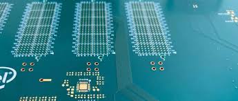
Megtron 7 PCB laminates are widely adopted in 5G servers, AI computing accelerators, and cloud networking equipment due to their exceptionally low dielectric loss and superior stability at 28–112 Gbps PAM4 and mmWave bands. As system architectures transition toward high-density multi-lane SerDes and advanced RF interconnects, PCB materials become a primary constraint influencing channel loss budgets, cross-talk behavior, and long-term reliability.
This article examines the dielectric advantages of Megtron 7, typical stackup strategies, RF simulation workflows, and practical engineering decisions in server backplane and high-speed computing module scenarios. A complete KKPCB case study is included with real-world measurements, stackup tables, and reliability test results.
Core Engineering Challenges
High-performance servers and computing modules introduce several design obstacles:
• Maintaining channel integrity at 56–112 Gbps PAM4 over long PCB routing distances
• Minimizing insertion loss and dielectric dissipation across Megtron 7 interconnect layers
• Achieving predictable impedance in dense routing regions with microvias and multi-layer transitions
• Limiting EMI leakage and mode conversion in hybrid RF/digital architectures
• Ensuring phase stability in high-frequency reference clocks and RF paths
• Securing mechanical and reliability robustness against thermal cycling during server operation
Megtron 7 PCB substrates address many of these challenges, but design quality depends heavily on stackup selection, hybrid material mixing, and precise RF modeling.
Material Science & Dielectric Performance
Megtron 7 laminates are engineered for high-speed and RF performance with ultra-low dielectric loss and stable electrical properties.
Table 1. Key Dielectric Parameters of Megtron 7
| Parameter | Typical Value | Notes |
|---|---|---|
| Dielectric Constant (Dk @ 10 GHz) | 3.4–3.45 | Stable across temperature & frequency |
| Dissipation Factor (Df @ 10 GHz) | 0.002–0.0025 | Extremely low-loss for 28–112 Gbps |
| Glass Transition Temperature (Tg) | ≥ 200 °C | Supports advanced reflow |
| CTE (Z-axis) | 45–55 ppm/°C | Reduces via fatigue |
| Thermal Conductivity | ~0.5 W/m·K | Balanced for computing systems |
| Moisture Absorption | ≤ 0.1% | Stabilizes RF and impedance parameters |
These properties enable consistent impedance control, reduced insertion loss, and excellent long-term phase behavior—essential for server-grade reliability.
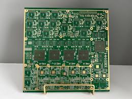
KKPCB Case Study — 5G Server Backplane and High-Speed Computing PCB
Application Background
A global cloud-computing server manufacturer required a multi-layer Megtron 7 PCB supporting 56 Gbps and 112 Gbps SerDes with strict channel-loss budgets. The board integrates:
• 5G fronthaul data interfaces
• High-speed CPU-to-accelerator interconnects
• Clock distribution networks at 25–50 GHz
• Dense via structures and hybrid RF/digital stackups
Engineering Problems Identified
• Excessive insertion loss near 40 GHz reference clock paths
• Resonance and impedance distortion at BGA breakout regions
• Risk of via-stub-induced reflections in long backplane routes
• Elevated differential skew in multi-lane paths
KKPCB Engineering Solutions
• Implemented Megtron 7 core-prepreg combinations optimized for differential-pair swing
• Introduced back-drilled vias to suppress stub resonance
• Performed HFSS-based 3D electromagnetic simulations for BGA escape channels
• Applied ADS channel simulation for PAM4 eye analysis
• Optimized copper roughness through low-profile foil selection
• Reinforced power-integrity planes with spread-resin prepregs to suppress resonant EMI
Measured Results
Table 2. Signal Integrity Measurement Results
Parameter |
Requirement |
Final Result |
Status |
|---|---|---|---|
| Insertion Loss @ 28 GHz | ≤ –1.5 dB/in | –1.28 dB/in | Passed |
| Insertion Loss @ 56 Gbps | Eye Mask 95% open | 97.6% open | Passed |
| TDR Impedance | 85 Ω ±10% | 84.7 Ω | Stable |
| Phase Variation | ≤ ±3° | ±2.1° | Passed |
| Near-End Crosstalk | < –40 dB | –42 dB | Passed |
The results confirm Megtron 7’s suitability for multi-GHz server workloads requiring both RF and ultra-high-speed digital coexistence.
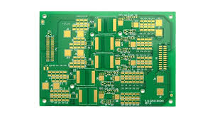
Stackup Design & RF Implementation
A typical optimized stackup is shown below.
Table 3. Megtron 7 PCB Stackup Example
Layer |
Material |
Thickness |
Function |
|---|---|---|---|
| L1 | Megtron 7 + LP Copper | 35 µm | High-speed routing |
| L2 | Megtron 7 Core | 100 µm | Ground reference |
| L3 | Megtron 7 | 60 µm | Differential pairs (28–56 Gbps) |
| L4 | Megtron 7 | 60 µm | Power/ground stability |
| L5 | Megtron 7 + LP Copper | 35 µm | RF paths & clock distribution |
RF Engineering Notes
• HFSS used for 3D electromagnetic modeling of vertical via-structures
• ADS for time-domain channel simulations and PAM4 eye diagrams
• TDR for post-fabrication impedance validation
• FEM thermal modeling to estimate hotspot behavior near CPU vicinity
These combined analyses ensure the PCB’s predictable performance under 5G and data-center workloads.
Environmental & Reliability Validation
To meet strict server-grade requirements, KKPCB applied a full reliability qualification plan.
Table 4. Reliability Test Summary
Test Item |
Condition |
Result |
|---|---|---|
| Thermal Cycling | –40 °C to +125 °C, 500 cycles | No via cracking |
| Humidity Resistance | 85 °C / 85% RH, 168 h | No electrical drift |
| Vibration Test | 10–500 Hz, 2 h per axis | Structural integrity stable |
| Solder Reflow | 260 °C, 3× cycles | No delamination |
| CAF Resistance | 100 V bias, 96 h | No failure |
Megtron 7’s low CTE and high Tg contributed significantly to the stable reliability profile.
Engineering Summary & Contact
Megtron 7 PCB substrates deliver outstanding performance for high-speed computing modules and advanced server backplanes. Their low-loss dielectric and stable electrical characteristics allow precise impedance control, reduced insertion loss, and reliable multi-GHz performance. Through optimized stackups, thorough RF simulation, and validated reliability testing, KKPCB enables high-performance 5G and data-center systems requiring consistent high-speed performance.
For engineering consultations, stackup planning, or RF/mmWave PCB fabrication, KKPCB provides end-to-end PCB solutions for global server and communication industries.
