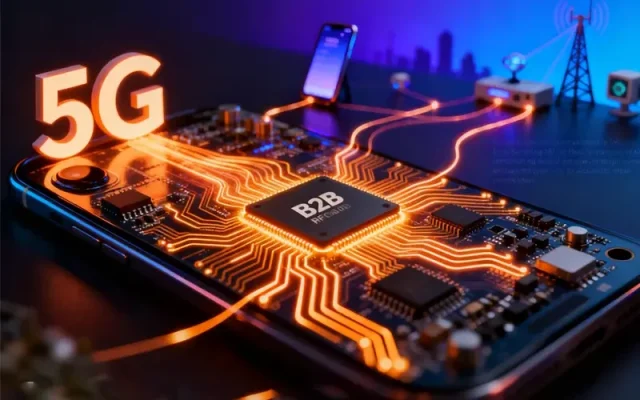
A 5G Router PCB is a high-performance printed circuit board designed to enable ultra-fast data transmission, low latency, and stable wireless connectivity in modern communication systems. Unlike traditional router boards, 5G routers must handle multi-gigabit data rates, high-frequency RF signals, and complex multi-antenna (MIMO) architectures.
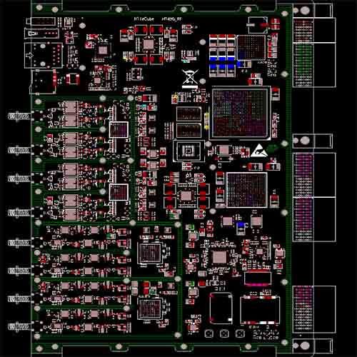
Typical 5G router PCB systems integrate:
-
RF front-end modules (power amplifiers, filters, transceivers)
-
Baseband processors and high-speed digital interfaces
-
Multi-layer antenna arrays
-
Power management and thermal control circuits
These requirements make 5G router PCBs among the most technically demanding designs in the networking industry.
Key Technical Challenges
Designing PCBs for 5G routers involves multiple engineering challenges:
-
High-Frequency Signal Integrity:
5G operates across sub-6 GHz and mmWave bands, requiring low-loss transmission and precise impedance control. -
High-Speed Digital Routing:
Interfaces such as PCIe, DDR, and Ethernet operate at multi-gigabit speeds, making signal integrity (SI) and power integrity (PI) critical. -
Massive MIMO Integration:
Multiple antennas increase routing density and introduce RF coupling and interference challenges. -
Thermal Management:
High data throughput and RF power levels generate significant heat, especially in compact router designs. -
EMI/EMC Compliance:
Dense RF and digital circuits increase electromagnetic interference risks, requiring careful shielding and grounding strategies.
PCB Design Architecture
To address these challenges, 5G router PCBs adopt advanced design architectures:
-
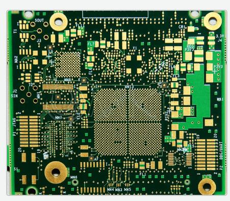
Multi-Layer Stack-Up (8–20+ Layers):
Separates RF, high-speed digital, power, and ground layers to minimize interference and ensure stable signal paths. -
Controlled Impedance Routing:
Microstrip, stripline, and coplanar waveguide structures are used for RF traces, while differential pairs are applied for high-speed digital signals. -
RF & Digital Isolation:
Physical and electrical separation between RF front-end and digital processing sections reduces noise coupling. -
Via Optimization:
Back-drilling and blind/buried vias minimize signal reflections and improve high-speed performance. -
Power Integrity Design:
Decoupling networks and low-impedance power planes stabilize voltage under dynamic load conditions.
Materials & Manufacturing
Material selection and fabrication precision are critical for 5G router PCBs:
-
Low-Loss Laminates:
Rogers, PTFE-based, Megtron, or hybrid materials are used to reduce dielectric loss and maintain signal integrity at high frequencies. -
Hybrid Stack-Ups:
Combining high-frequency materials with FR-4 balances performance and cost. -
High-Precision Fabrication:
Tight control of trace width, spacing, and dielectric thickness ensures consistent impedance. -
Surface Finishes:
ENIG or immersion silver supports high-frequency performance and reliable assembly. -
Quality Assurance:
-
Impedance testing and TDR for high-speed traces
-
VNA testing for RF performance
-
AOI/X-ray inspection for multilayer alignment
-
Thermal and environmental testing for long-term reliability
-
KKPCB leverages advanced manufacturing capabilities to deliver high-reliability 5G router PCBs that meet stringent communication standards.
Application Insights
5G router PCBs are widely deployed across modern communication infrastructure:
-
Consumer 5G Routers: High-speed home and enterprise connectivity devices
-
Telecom Infrastructure: Base stations and edge networking equipment
-
Industrial IoT Gateways: Reliable high-speed connectivity for smart factories
-
Mobile Hotspot Devices: Compact routers with high data throughput
-
Smart City Networks: Supporting large-scale connected systems
As 5G technology continues to evolve, PCB design must keep pace with increasing frequency, bandwidth, and integration complexity. By combining advanced materials, precise layout, thermal management, and rigorous QA, KKPCB delivers 5G Router PCBs capable of supporting next-generation wireless communication systems.
