Why mmWave Changes Everything

The transition from sub-6 GHz to millimeter wave (mmWave) frequencies fundamentally changes PCB design. Operating typically between 24 GHz and 100 GHz+, mmWave systems push PCB technology to its limits.
At these frequencies, the PCB is no longer just a passive interconnect—it becomes an active part of the RF system, directly affecting signal propagation, radiation, and overall system efficiency.
Even minor variations in trace geometry, material properties, or surface roughness can significantly impact performance. This makes mmWave PCB design a precision-driven engineering discipline.
Frequency Challenges at mmWave
Designing for mmWave introduces challenges far beyond traditional RF:
- Severe Signal Loss:
Conductor loss and dielectric loss increase dramatically with frequency, requiring ultra-low-loss materials and short transmission paths. - Surface Roughness Effects:
At mmWave frequencies, current flows primarily on the conductor surface, making copper roughness a major contributor to signal attenuation. - Tight Tolerances:
Small dimensional variations can lead to impedance mismatch and phase errors. - Radiation & Coupling:
Unintended radiation and coupling between traces become more pronounced, affecting signal integrity. - Thermal Density:
High-frequency ICs and power amplifiers generate localized heat, requiring efficient thermal management.
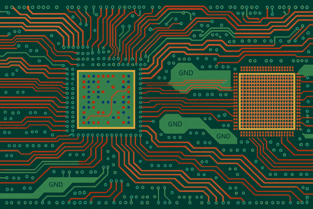
PCB Architecture Strategy
To address these challenges, mmWave PCBs adopt highly optimized architectures:
- Short RF Paths:
Minimizing trace length reduces insertion loss and signal degradation. - Antenna-in-Package (AiP) Integration:
Antennas are often integrated directly with the PCB or package to reduce interconnect losses. - Layer Isolation:
RF layers are isolated from digital and power layers to prevent interference. - Advanced Via Structures:
Back-drilling, microvias, and via fences reduce signal discontinuities and improve grounding. - Controlled Impedance & Phase Matching:
Critical for beamforming and phased array systems used in 5G mmWave.
This architecture ensures that the PCB supports both signal transmission and RF radiation efficiency.
Materials & Loss Control
Material selection is one of the most critical decisions in mmWave PCB design:
- Ultra-Low-Loss Laminates:
Materials such as PTFE-based laminates, hydrocarbon ceramic composites, and advanced low-loss systems (e.g., Rogers, Taconic, Megtron) are commonly used. - Stable Dielectric Constant (Dk):
Consistency across frequency and temperature ensures reliable impedance and phase behavior. - Low Dissipation Factor (Df):
Essential to minimize insertion loss at mmWave frequencies. - Smooth Copper Foil:
Low-profile or ultra-smooth copper reduces conductor loss. - Hybrid Stack-Ups:
Combining high-frequency materials with FR-4 helps balance cost and performance.
At mmWave frequencies, material choice directly determines system efficiency and range.
Manufacturing & Validation
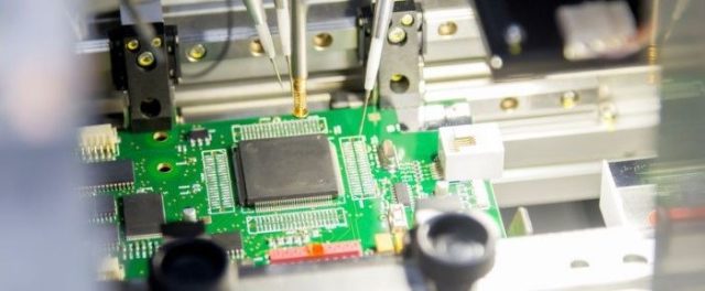
mmWave PCBs require extremely tight fabrication control and advanced validation methods:
- Precision Fabrication:
Tight tolerances on trace width, spacing, and dielectric thickness are essential. - Surface Finish Selection:
ENIG or immersion silver is preferred to maintain conductivity and minimize surface loss. - Advanced Inspection:
- X-ray inspection for via integrity
- AOI for fine line accuracy
- Cross-section analysis for stack-up validation
- High-Frequency Testing:
- Time Domain Reflectometry (TDR) for impedance
- Vector Network Analysis (VNA) for insertion/return loss
- mmWave over-the-air (OTA) testing for antenna performance
At KKPCB, we apply strict process control to ensure mmWave PCBs meet ultra-high-frequency performance requirements.
Where It’s Used
5G mmWave PCBs are deployed in cutting-edge applications where high bandwidth and ultra-low latency are required:
- 5G Base Stations (mmWave small cells)
- Phased Array Antenna Systems
- High-Speed Wireless Backhaul
- Autonomous Driving Radar Systems
- Advanced Aerospace & Defense Communication Systems
These applications rely on PCBs that can support precise RF behavior at extremely high frequencies, where traditional PCB design approaches are no longer sufficient.
Final Thoughts
5G mmWave PCBs represent the frontier of PCB engineering, where materials science, RF design, and manufacturing precision converge. Success at these frequencies depends on controlling every variable—from dielectric properties to copper surface roughness.
By combining advanced materials, optimized RF architectures, and precision manufacturing, KKPCB delivers 5G mmWave PCBs that enable next-generation wireless communication systems to perform reliably and efficiently.
