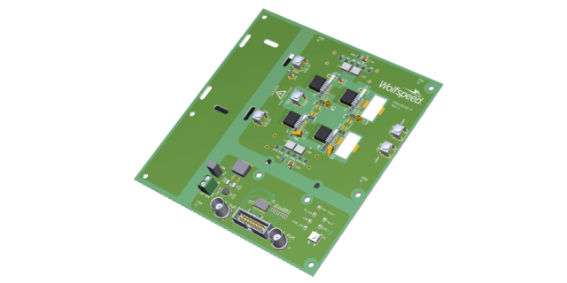
Silicon carbide (SiC) power devices have transformed modern power electronics, enabling ultra-efficient, high-voltage, and high-temperature operation in electric vehicles, high-power converters, charging stations, aerospace systems, and industrial automation. As SiC MOSFETs and SiC Schottky diodes continue to push switching speeds and power densities upward, SiC PCB technologies become essential for supporting these devices with stable thermal, electrical, and mechanical performance.
A SiC PCB is not simply a traditional board with SiC components placed on top; it is a specialized high-performance substrate engineered to handle the thermal stress, dielectric requirements, and high-voltage isolation demanded by wide-bandgap power devices. These boards often incorporate ceramic substrates, insulated metal substrates (IMS), or advanced copper-ceramic bonding to unlock the full performance of SiC devices.
1. Why SiC PCB Is Critical for High-Power and High-Temperature Operation
SiC semiconductors operate efficiently at >600 V, switch extremely fast, and tolerate junction temperatures approaching 200–250°C. Conventional FR-4 or mid-loss laminates cannot survive such harsh conditions. SiC PCB architectures overcome these limitations through:
• exceptional thermal conductivity (20–170 W/m·K depending on ceramic/IMS stackup)
• high dielectric strength ensuring safe insulation above 1–5 kV
• low parasitic inductance improving switching efficiency
• stable performance under thermal cycling and mechanical shock
These properties allow power inverters, DC-DC converters, high-current battery systems, and motor drives to run at high efficiency without thermal runaway or insulation breakdown.
2. Material Architectures in SiC PCB Engineering
High-performance SiC PCB designs rely on advanced substrate technologies, each optimized for extreme environments:
AlN (Aluminum Nitride) Ceramics
• Thermal conductivity up to 170 W/m·K
• Low CTE mismatch with SiC chips
• Excellent dielectric reliability
AlN-based SiC PCBs are common in EV inverter modules, aviation power systems, and industrial motor drives.
Al₂O₃ (Alumina) Ceramics
• Cost-efficient ceramic PCB option
• Thermal conductivity 18–30 W/m·K
• High dielectric insulation
Used for medium-power SiC converter circuits and power distribution modules.
Insulated Metal Substrate (IMS)
• Aluminum or copper baseplate for direct heat spreading
• Typically paired with SiC MOSFET modules
• Supports high currents and aggressive switching
A preferred choice for fast chargers, renewable-energy inverters, and power control units (PCUs).
DBC and AMB Copper-Ceramic Technologies
Direct Bonded Copper (DBC) and Active Metal Brazed (AMB) substrates deliver:
• large copper thickness
• high reliability under thermal cycling
• strong bonding with ceramic cores
They serve as the backbone of SiC half-bridge and full-bridge power modules.
3. High-Frequency, Low-Loss Power Routing in SiC PCB Designs
The fast switching capabilities of SiC devices bring significant electromagnetic challenges. Proper SiC PCB engineering addresses:
• low loop inductance for cleaner switching transitions
• minimized EMI through optimized copper geometry
• controlled parasitic capacitance to reduce dv/dt stress
• short, wide traces for high-current paths
High-speed SiC converters operating at 50–500 kHz require extremely low parasitic behavior to maintain efficiency and reduce switching losses. SiC PCBs with copper-ceramic bonding maintain stable electrical parameters even under rapid transient loads.
4. Thermal Management and Heat Extraction Strategies
SiC PCBs excel in harsh thermal environments. Effective heat extraction within SiC PCB assemblies includes:
• metal-backed substrates (Al/Cu) for heat spreading
• ceramic cores preventing dielectric degradation
• thick copper (2–6 oz) for high-current conduction
• direct-attach die (DAD) for minimal thermal resistance
Because SiC chips routinely operate above 175°C, SiC PCBs must retain structural rigidity and insulation without delamination, blistering, or drift in dielectric properties.
Heat reliability is especially critical in EV traction inverters, onboard chargers (OBC), solar inverters, and aerospace power conditioning systems.
5. High-Voltage Insulation and Safety Performance
SiC PCB structures support stringent high-voltage insulation through:
• wide creepage and clearance calculated for 800–1500 V systems
• ceramic substrates with high dielectric breakdown (15–30 kV/mm)
• multi-layer isolation with IMS or DBC
The superior insulation characteristics of SiC PCB materials ensure long-term safety in:
• EV battery management and high-voltage switching
• industrial automation drives
• grid-connected power converters
• rail power systems
SiC PCB insulation stability under humidity, vibration, and continuous thermal stress is a decisive factor behind SiC adoption in mission-critical electronics.
6. Mechanical Reliability and Long-Term Durability
SiC PCBs must survive demanding mechanical loads, including:
• high vibration in EVs and aerospace
• thousands of thermal cycles in grid power systems
• heavy solder joint stress from high-current devices
DBC and AMB SiC substrates are particularly valued for their low CTE mismatch with SiC dies, preventing cracking or solder joint fatigue during long-term operation.
Conclusion
SiC PCB engineering enables the next generation of high-power, high-temperature, and high-efficiency electronic systems. With unparalleled thermal conductivity, dielectric reliability, low inductance, and mechanical robustness, SiC PCBs form the backbone of modern power electronics—from electric vehicles to renewable energy, aerospace, and industrial automation.
As wide-bandgap technologies continue advancing, SiC PCBs will play an even greater role in unlocking higher power density, faster switching, and more compact, reliable high-voltage systems.
