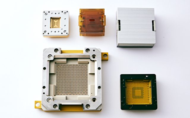
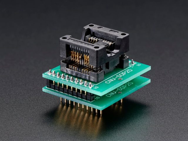
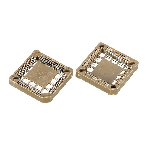
A Test Socket PCB for IC is a specialized semiconductor test PCB used to mount and interface IC test sockets within Automated Test Equipment (ATE) systems. Acting as the electrical bridge between the tester and the device under test (DUT), the test socket PCB ensures reliable signal transmission, stable power delivery, and consistent mechanical alignment during IC validation and production testing.
As modern ICs evolve toward higher pin counts, finer pitch packages, and higher-speed operation, the design and manufacturing of test socket PCBs for ICs have become increasingly critical to overall test accuracy and yield.
Key Design Requirements of Test Socket PCBs for ICs
1. High Pin Count and Fine-Pitch Routing
IC test sockets often accommodate BGA, QFN, LGA, and CSP packages with dense I/O configurations. Test socket PCBs require fine-line routing, HDI structures, and multilayer stackups to support these high pin count devices.
2. Controlled Impedance and Signal Integrity
High-speed digital and RF IC testing demands strict controlled impedance PCB design. Proper stackup planning and trace geometry minimize signal reflection, skew, and crosstalk between socket pins.
3. Mechanical Accuracy and Socket Alignment
Precise pad positioning and PCB flatness are essential to maintain reliable electrical contact between the IC and the test socket during repeated insertion cycles.
4. Power Integrity and Noise Control
Stable power delivery ensures accurate IC performance measurements. Optimized power and ground planes, along with effective decoupling, reduce voltage fluctuation and electrical noise.
5. Durability for Repeated Test Cycles
Test socket PCBs must withstand frequent IC insertions and removals. Robust materials and controlled manufacturing tolerances ensure long service life and consistent performance.
Applications of Test Socket PCBs for ICs
Test socket PCBs are widely used in:
-
Logic IC and microprocessor testing
-
Memory IC testing (DRAM, NAND, Flash)
-
RF and mixed-signal IC validation
-
Automotive and industrial IC testing
-
High-reliability semiconductor production environments
These applications require stable contact performance and repeatable electrical behavior.
Manufacturing Capabilities for Test Socket PCBs
Producing reliable test socket PCBs for ICs requires advanced manufacturing capabilities, including:
-
HDI and multilayer PCB fabrication
-
Controlled impedance manufacturing and verification
-
Precision drilling and fine-line etching
-
High-Tg and low-loss laminate processing
-
Prototype, small batch, and volume production support
Advanced manufacturing ensures consistent electrical and mechanical performance across different test platforms.
Why Test Socket PCB Quality Matters
A low-quality test socket PCB can cause intermittent contact, signal distortion, and unstable measurements, leading to false test results and reduced yield. High-quality test socket PCBs provide:
-
Reliable electrical contact over repeated cycles
-
Accurate signal and power delivery
-
Reduced test downtime and socket wear
-
Improved ATE efficiency and throughput
Conclusion
The Test Socket PCB for IC is a critical component in semiconductor testing, providing the mechanical and electrical foundation for accurate IC validation. Through HDI routing, controlled impedance design, precise socket alignment, and robust manufacturing, these PCBs ensure stable, repeatable, and high-accuracy test performance.
Partnering with an experienced test socket PCB manufacturer helps improve test reliability, reduce maintenance costs, and support advanced semiconductor testing requirements.
