
Many radar and sensing assemblies combine a high-frequency channel with digital control, power conversion, and dense connectors. A hybrid construction can reduce cost and routing pressure, but only when the RF laminate, FR-4 regions, and transition references are engineered as one system. This guide uses the RO4835 PCB as the RF element in an illustrative hybrid stackup.
Why a hybrid stackup needs a systems decision
The RO4835 PCB layer plan should show which layers carry RF, which layers carry digital buses, and where the material transition occurs. Do not let a cost-down substitution change the reference height under a critical line. Freeze finished dielectric assumptions and copper treatment before routing both domains.
| Hybrid decision | Risk if implicit | Control before release |
|---|---|---|
| RF laminate location | Unknown impedance reference | Assign signal and return layers explicitly |
| FR-4 digital zone | Unplanned crosstalk | Set keep-outs and return stitching |
| Material interface | Resin or press variation | Release construction and lamination notes |
| Connector transition | Launch discontinuity | Review footprint with both stackup regions |
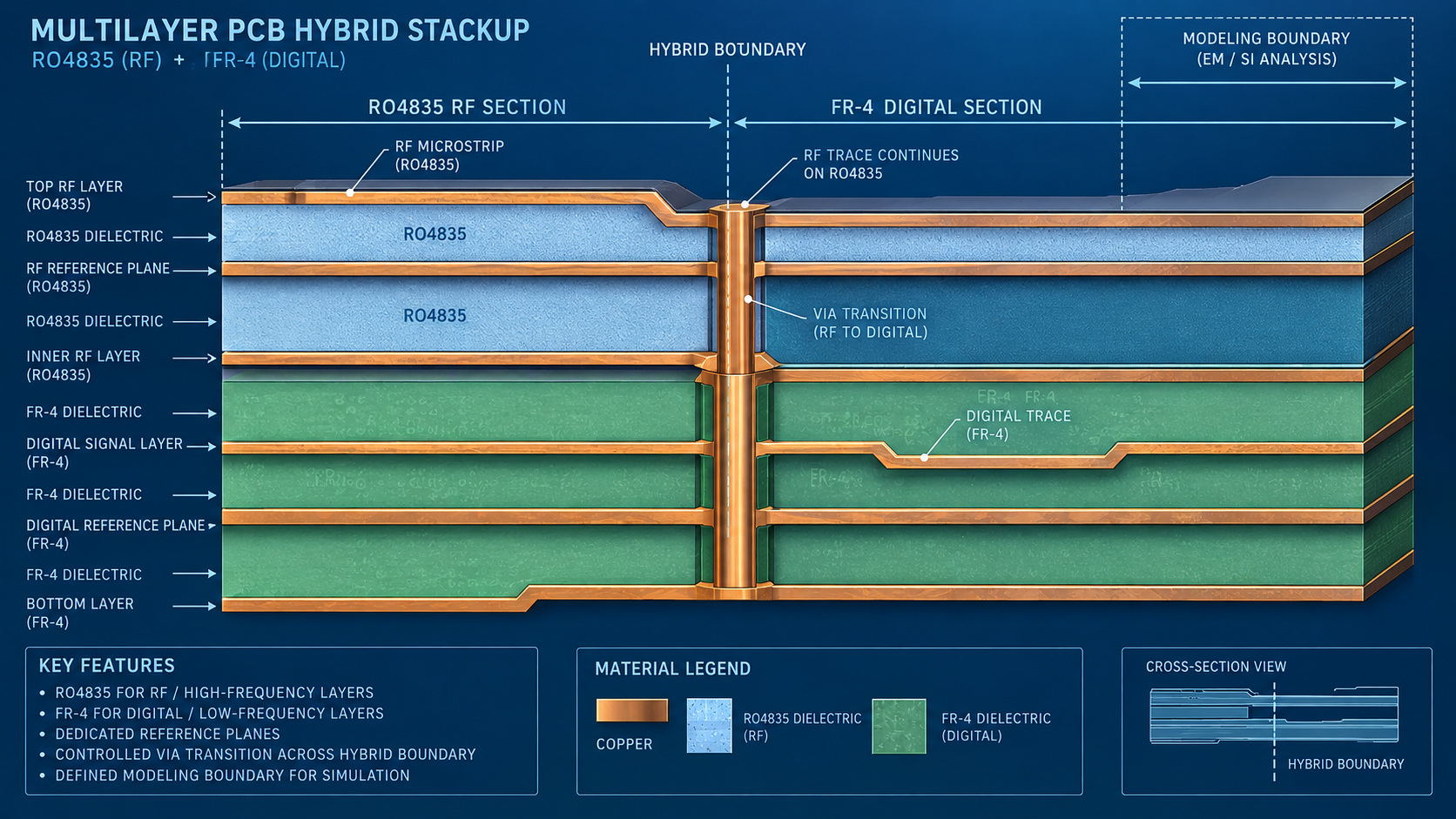
Illustrative hybrid material stackup separating RF reference layers from digital routing layers.
Keep the RF and digital return paths intentional
A hybrid multilayer PCB is not a license to leave ground stitching until the end. Place return vias around connector fields, define digital-region keep-outs, and check every layer transition. The RF section should maintain a continuous reference while digital power planes remain balanced and manufacturable.
Interface review checklist
- Mark the material boundary and its mechanical datum in the layout.
- Keep critical RF lines away from uncontrolled resin transitions.
- Provide nearby return vias at every connector and layer change.
- Check digital plane splits for unwanted RF return detours.
- Document which impedance values are calculated and which are measured.
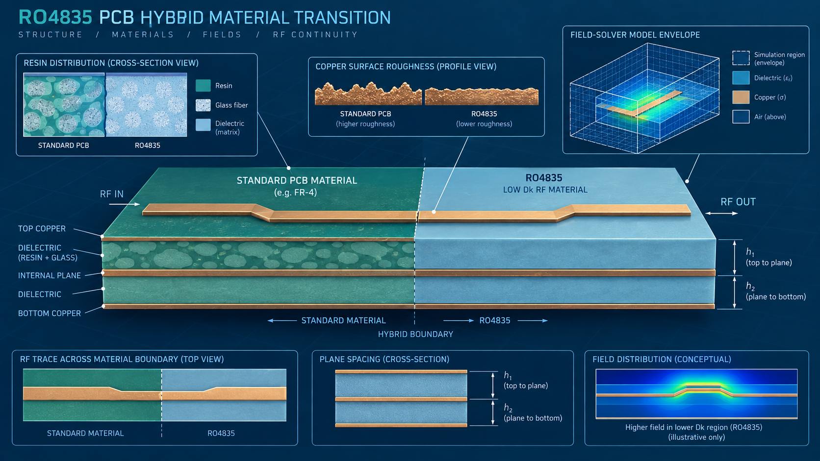
Illustrative resin and copper transition concept for a mixed RF–digital board.
Review material compatibility and fabrication sequence
The PCB manufacturing review should confirm press-cycle compatibility, copper balance, drilling rules, and registration across the hybrid build. A PCB materials substitution must be evaluated against finished thickness and the complete RF path, not just a nominal dielectric constant.
- Confirm the approved laminate and resin system for every layer group.
- Check copper distribution to limit panel bow and twist.
- Verify drill, backdrill, and annular-ring rules at material boundaries.
- Align solder-mask and surface-finish notes with both RF and digital pads.
- Route every deviation through an ECO with a named owner.
Example sign-off for an RF–digital module
In an illustrative program, the RO4835 PCB release can require stackup approval, field-solver review, connector launch inspection, and a coupon plan before purchasing places the build. The HDI PCB option should only be selected when its microvia and sequential-lamination requirements are explicit. These gates distinguish design targets from project-specific test evidence.
Questions from design and sourcing teams
Can the RF laminate be replaced with any low-loss material?
No. Recheck dielectric height, copper treatment, press behavior, and the launch model for the proposed construction.
Should digital planes cross the material interface?
Only with a defined return strategy. Review plane continuity, stitching, and noise coupling at the boundary.
What belongs on the fabrication drawing?
Include the material map, stackup revision, impedance intent, drill rules, copper class, and deviation authority.
Sources: Vendor-typical RO4835 material context and KKPCB public High-Frequency PCB, PCB Materials, Multilayer PCB, HDI PCB, and PCB Manufacturing categories. No external hyperlinks or claimed customer measurements are used.
For the final RO4835 PCB release, keep the RO4835 PCB hybrid layer map, material approvals, transition notes, and inspection plan under one revision.
Keep the RO4835 PCB hybrid stackup, RO4835 PCB material map, RO4835 PCB RF reference, RO4835 PCB return path, RO4835 PCB transition notes, RO4835 PCB coupon, RO4835 PCB inspection plan, and RO4835 PCB deviation record under one controlled revision.
