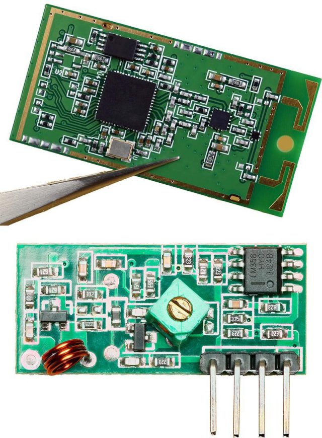
An RF IC Test PCB is a specialized semiconductor test circuit board designed to evaluate the electrical performance of radio frequency integrated circuits during wafer-level, package-level, or final testing stages. It is a critical interface within Automated Test Equipment (ATE) systems, enabling accurate measurement of RF parameters such as gain, noise figure, phase noise, insertion loss, and linearity.
As RF ICs are widely used in 5G communication, IoT devices, automotive radar, wireless modules, and microwave systems, RF IC test PCBs must deliver excellent signal integrity, low loss transmission, and stable impedance control across high-frequency bands.
Key Design Requirements of RF IC Test PCBs
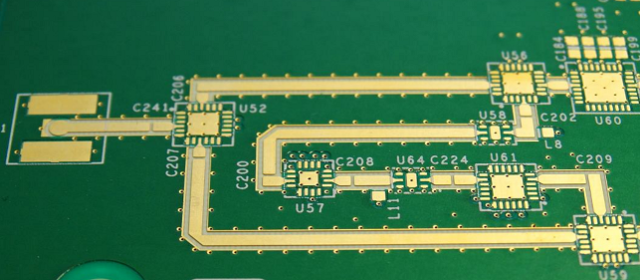
1. Controlled Impedance for RF Signals
RF IC test PCBs require precise 50Ω / 75Ω controlled impedance routing to minimize signal reflection and measurement errors. Stackup design, dielectric thickness, and trace geometry must be tightly controlled.
2. Low-Loss Materials for High-Frequency Performance
To reduce insertion loss and phase distortion, RF IC test PCBs commonly use low-Dk and low-Df materials. These materials ensure stable signal transmission at GHz and mmWave frequencies.
3. High-Frequency Signal Integrity
RF test environments demand strict control over crosstalk, EMI, return loss, and signal attenuation. Optimized ground referencing, short signal paths, and isolation structures are essential for accurate RF testing.
4. High Pin Count and Dense Interconnects
Modern RF ICs often integrate digital, analog, and RF functions in a single package. HDI PCB technology, fine-line routing, and microvias enable efficient fanout while maintaining RF performance.
5. Mechanical Precision and Connector Compatibility
RF IC test PCBs must provide precise pad alignment and flatness to ensure reliable contact with RF connectors, probes, and test sockets, maintaining consistency across repeated test cycles.
Applications of RF IC Test PCBs
RF IC test PCBs are widely used in:
-
5G and wireless communication IC testing
-
RF front-end module validation
-
IoT and smart device RF testing
-
Automotive radar and V2X IC testing
-
Microwave and mmWave semiconductor evaluation
Each application relies on accurate RF measurements and repeatable test conditions.
Manufacturing Requirements for RF IC Test PCBs
High-performance RF IC test PCBs demand advanced manufacturing capabilities, including:
-
Controlled impedance multilayer PCB fabrication
-
Fine-line and HDI processing
-
Low-loss laminate handling
-
Precision drilling and via control
-
Impedance testing and RF performance verification
These processes ensure consistent electrical performance and long-term reliability.
Why RF IC Test PCB Quality Is Critical
Poorly designed RF IC test PCBs can result in:
-
Signal reflection and excessive insertion loss
-
Inaccurate RF measurements and false test results
-
Increased noise and EMI interference
-
Reduced test efficiency and lower yield
A high-quality RF IC test PCB ensures accurate RF characterization, stable test conditions, and high measurement repeatability.
Conclusion
The RF IC Test PCB plays a vital role in high-frequency semiconductor testing, enabling precise evaluation of RF and microwave ICs. By combining controlled impedance design, low-loss materials, HDI routing, and precision manufacturing, RF IC test PCBs deliver reliable and repeatable test results across demanding RF applications.
Choosing an experienced RF IC test PCB manufacturer helps ensure measurement accuracy, testing efficiency, and long-term reliability for advanced wireless, automotive, and high-frequency semiconductor systems.
