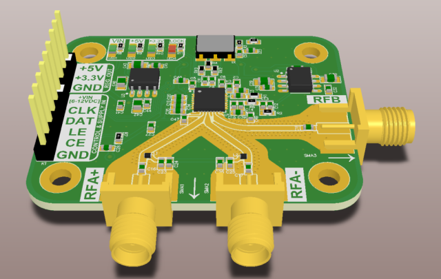
With the rapid growth of 5G, IoT, and wireless communication technologies, RF ICs have become increasingly complex and high-speed. Ensuring the performance and reliability of RF and microwave chips requires specialized IC test PCBs that can handle high-frequency signals while maintaining signal integrity and precise mechanical alignment.
RF IC Test PCBs provide the critical interface between RF chips and automated test equipment (ATE) or probe cards, enabling accurate functional testing, parametric measurements, and wafer-level validation.
What Is an RF IC Test PCB?
An RF IC Test PCB is a high-performance printed circuit board designed specifically for testing RF and microwave integrated circuits. Its main functions include:
-
Routing high-frequency signals from IC pads to ATE or probe cards
-
Maintaining controlled impedance to preserve RF signal integrity
-
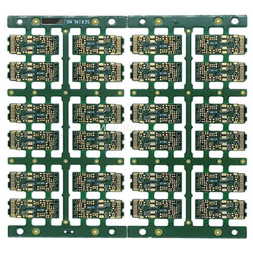
Supporting fine-pitch, high-pin-count RF IC packages
-
Providing mechanical stability for accurate probe alignment
-
Reducing signal loss, reflections, and crosstalk
These PCBs are critical for reliable, repeatable, and accurate RF IC testing.
Key Features of RF IC Test PCBs
-
Controlled Impedance
Ensures high-frequency signal integrity and accurate RF measurement. -
High-Density Routing
Supports modern RF ICs with hundreds or thousands of I/O pins. -
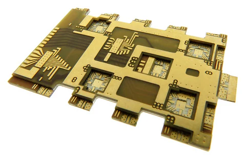
Multilayer and HDI Structures
Optimizes routing for high-speed signals while separating power and ground planes. -
Low-Loss Materials
Uses laminates like Rogers, Taconic RF-35, or Duroid 5880 to minimize insertion loss and maintain RF performance. -
Mechanical Precision
Accurate probe card or socket alignment ensures consistent and repeatable test results.
Materials and Stackup for RF IC Test PCB
Selecting the proper material and stackup is critical for RF IC testing:
-
Low-loss RF laminates (Rogers, Taconic, Duroid) for minimal signal attenuation
-
High-Tg FR-4 for mixed-signal applications
-
Hybrid stackups for designs combining RF and digital signals
-
Thermally stable cores for long burn-in or high-power testing
The right material and stackup ensure signal integrity, low insertion loss, and dimensional stability during high-frequency testing.
Applications of RF IC Test PCBs
RF IC test PCBs are widely used in:
-
5G, Wi-Fi, and mmWave IC functional and parametric testing
-
Wafer-level and package-level RF validation
-
Probe card and load board interfaces in ATE systems
-
Prototype testing for RF ICs and high-speed communication chips
-
Small-batch and pilot production verification
These applications demand precision, high-speed performance, and repeatable results, all enabled by specialized RF IC test PCBs.
Choosing a RF IC Test PCB Manufacturer
Selecting the right RF IC test PCB partner is critical for maintaining measurement accuracy and project schedules. Key criteria include:
-
Expertise in high-frequency, controlled-impedance PCB design
-
Ability to manufacture HDI, multilayer, and high-pin-count boards
-
Experience with low-loss RF materials and hybrid stackups
-
Support for prototype, small-batch, and volume production
-
Strong engineering and quality control processes
A professional partner ensures reliable, repeatable RF IC testing across multiple projects.
Conclusion
RF IC Test PCBs are essential for high-frequency chip validation, providing controlled impedance, high-density routing, and mechanical precision. Partnering with an experienced manufacturer ensures accurate RF and microwave IC testing, faster design validation, and smoother transition to volume production for wireless and communication applications.
