What Is a PTFE PCB?
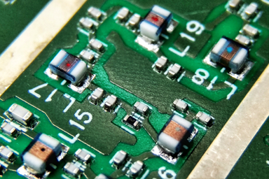
A PTFE PCB is a high-performance RF PCB built using PTFE material (Polytetrafluoroethylene), engineered for ultra-low signal loss and stable high-frequency performance.
PTFE PCB materials are widely used in microwave, RF, and mmWave PCB designs, where traditional materials cannot maintain signal integrity.
Key characteristics of PTFE PCB materials include:
- Very low dielectric constant (Dk)
- Extremely low dissipation factor (Df)
- Excellent frequency stability
- High thermal and chemical resistance
In advanced RF PCB design, PTFE PCB materials are often the benchmark for low-loss performance.
Why PTFE PCB Materials Are Critical in RF Design
The main advantage of PTFE PCB lies in its superior electrical properties:
- Ultra-Low Loss (Df):
Minimizes signal attenuation in RF traces - Stable Dielectric Constant (Dk):
Ensures consistent impedance across frequency ranges - High-Frequency Capability:
Suitable for GHz to mmWave applications - Excellent Signal Integrity:
Supports long-distance RF signal transmission - Low Dispersion:
Maintains signal phase stability
These properties make PTFE PCB essential for high-frequency RF PCB applications where precision matters.
PTFE PCB vs Other RF PCB Materials
When comparing PTFE PCB with other RF PCB materials (such as hydrocarbon or FR-4), the differences become clear:
| Property | PTFE PCB | Rogers PCB | FR-4 PCB |
|---|---|---|---|
| Loss (Df) | Ultra Low | Low | Higher |
| Dk Stability | Excellent | Very Good | Moderate |
| Frequency Range | mmWave | GHz | Low-Mid |
| Processing Difficulty | High | Medium | Low |
| Cost | Highest | High | Low |
Key Insight:PTFE PCB delivers the best performance—but also the highest complexity and cost.
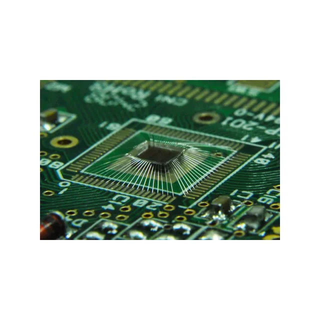
Manufacturing Challenges of PTFE PCBs
While PTFE PCB offers excellent electrical performance, it is difficult to manufacture:
- Soft Material Structure:
PTFE is mechanically soft, making drilling and handling challenging - Poor Adhesion:
Copper bonding requires special surface treatment - Dimensional Instability:
Material expansion can affect registration accuracy - Drilling Complexity:
Requires controlled processes to avoid deformation - Lamination Challenges:
PTFE layers require precise temperature and pressure control
Not all PCB manufacturers can reliably produce high-quality PTFE PCBs.
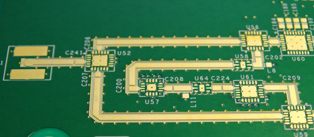
PTFE PCB Design Best Practices
To fully leverage PTFE PCB performance, careful design is required:
- Controlled Impedance RF Trace Design
Ensure precise RF trace geometry for stable impedance - Minimize RF Trace Length
Reduce insertion loss in high-frequency paths - Limit Via Usage
Vias introduce discontinuities in RF PCB design - Use Smooth Copper Foil
Reduces conductor loss in PTFE PCB - Optimize Stack-Up Design
Consider hybrid structures to balance cost - Ensure Strong Grounding
Continuous ground planes improve RF performance
In PTFE PCB design, layout quality directly impacts RF performance.
When Should You Use a PTFE PCB?
PTFE PCB is necessary when performance requirements are extremely high:
Use PTFE PCB when:
- Designing mmWave systems (e.g., 24GHz, 77GHz radar)
- Developing high-frequency RF front-end modules
- Building satellite communication systems
- Requiring ultra-low signal loss
- Working with precision RF measurement systems
Avoid PTFE PCB when:
- Frequency is below 1 GHz
- Cost constraints are strict
- Rogers or other RF materials can meet requirements
Engineering principle:Use PTFE PCB only when its performance advantage is truly needed.
Cost Optimization: Hybrid PTFE PCB
To reduce cost, many designs adopt a hybrid PTFE PCB approach:
- PTFE material for RF signal layers
- FR-4 or other materials for non-critical layers
Benefits:
- Lower overall PCB cost
- Maintained RF performance
- Improved manufacturability
Hybrid stack-ups are widely used in commercial RF PCB designs.
Common Mistakes in PTFE PCB Design
Avoid these typical PTFE PCB design errors:
- Treating PTFE PCB like standard FR-4
- Ignoring manufacturing constraints
- Overusing PTFE material unnecessarily
- Poor impedance control in RF traces
- Inadequate grounding design
These mistakes can significantly reduce the effectiveness of PTFE PCB.
Final Thoughts
PTFE PCBs represent the highest level of RF PCB material performance, offering ultra-low loss and exceptional high-frequency stability.
However, successful PTFE PCB implementation requires:
- Advanced RF design expertise
- Careful material selection
- Manufacturing-aware design
- Cost-performance optimization
At KKPCB, we provide PTFE PCB manufacturing and RF design support, ensuring your high-frequency designs achieve maximum performance, reliability, and efficiency.
