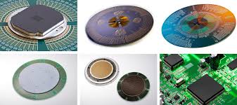
Probe Card PCB: Engineering Precision for Wafer-Level Testing
Introduction
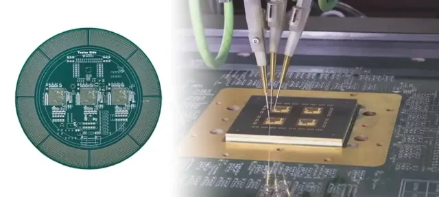
At the wafer-level test stage, the probe card PCB serves as the indispensable interface between automated test equipment (ATE) and the semiconductor wafer. As device geometries continue shrinking and electrical performance requirements become more demanding, precision test interfaces have become essential. The probe card PCB establishes reliable electrical connectivity between densely packed probe needles and ATE systems, enabling IC manufacturers to validate die functionality before dicing and packaging.
What Is a Probe Card PCB?
Definition and Core Function
A probe card PCB is a high-precision, application-specific printed circuit board used to route signals, power, and ground between the ATE and the probe needle array. It must maintain electrical accuracy across hundreds to tens of thousands of contact points while providing mechanical stability for wafer probing operations. Functionally, it acts as both:
-
an electrical distribution network for high-speed and precision test signals, and
-
a mechanical platform that aligns probes with micrometer-scale accuracy to the die pads.
Key Components
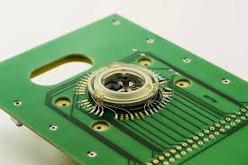
A complete probe card PCB assembly typically includes:
-
Probe needle array – Contacts wafer die pads with ultra-fine pitch.
-
PCB interface layers – High-density routing with impedance-controlled traces.
-
ATE connectors – Customized high-pin-count interfaces for system-level integration.
-
Mechanical support structures – Ensures planarity, rigidity, and repeatable probing.
These elements must operate in unison to achieve consistent electrical contact with die pad pitches often below 100 μm.
Probe Card PCB vs. Load Board PCB
| Aspect | Probe Card PCB | Load Board PCB |
|---|---|---|
| Test Stage | Wafer-level | Package-level |
| Connection Target | Bare die | Packaged IC |
| Design Focus | Alignment, SI, fine pitch | Current, thermal, mixed signals |
| Pitch Requirements | Ultra-fine (<100 μm) | Standard package pitch |
Structural Design of Probe Card PCBs
Multi-Layer Stack-Up Architecture
Probe card PCBs frequently require 6 to 20+ layers to support dense routing, controlled impedance, and shielding structures. Typical laminate choices include:
-
High-Tg FR-4 – Cost-effective for moderate frequencies
-
BT resin – Low CTE and stable electrical behavior
-
Rogers 4000 series – For high-frequency (>10 GHz) and low-loss requirements
Stack-ups incorporate isolated signal layers, continuous ground planes, and robust power structures to ensure clean, repeatable measurements.
Advanced Via Technologies
Miniaturized probe pitches demand aggressive HDI methods:
-
Laser-drilled microvias (≈75 μm) for high-density routing
-
Blind and buried vias to interconnect inner layers without surface space loss
-
Via-in-pad for ultra-fine probe pad geometries and minimized parasitics
These technologies enable reliable routing for thousands of densely spaced signals.
Impedance Control
Probe card PCBs typically require:
-
50 Ω single-ended lines
-
100 Ω differential pairs
To achieve this, layer thicknesses must be controlled within ±10%, and ground planes positioned to ensure low-inductance return paths. Proper impedance control reduces reflections, improves signal fidelity, and ensures measurement accuracy.
Fine-Pitch & High-Frequency Design Challenges
Ultra-Fine Pitch Requirements
Modern semiconductor devices may demand probe pitches <50 μm, requiring:
-
Registration accuracy <25 μm across the entire panel
-
High-precision imaging and alignment systems
-
Thermal expansion compensation during fabrication
Any deviation affects probe alignment, risking damage or failed contact.
High-Frequency Signal Integrity
For devices above 10 GHz, the probe card PCB must address:
-
Skin-effect losses
-
Dielectric absorption
-
Impedance discontinuities
-
Crosstalk in densely routed layouts
Low-loss laminates (Df < 0.004), well-matched differential pairs, and precise length-matching (<1 mm) are crucial.
Crosstalk Mitigation
Techniques include:
-
Ground-Signal-Ground (GSG) routing
-
Embedded capacitance materials for local decoupling
-
Solid reference planes to prevent electromagnetic coupling
These strategies preserve signal fidelity even in dense probe fields.
ATE System Interface
Platform-Specific Integration
Probe card PCBs must meet the mechanical and electrical requirements of major ATE platforms such as:
-
Advantest V93000
-
Teradyne UltraFlex
-
Cohu / Verigy systems
Connectors must align thousands of channels with probe contact locations via customized signal mappings and mechanical docking precision.
Ground Architecture
A robust grounding scheme ensures:
-
Low-noise operation
-
Accurate parametric measurements
-
Reduced ground impedance
Multiple ground pins and uniform ground planes eliminate ground loops and minimize noise injection.
Durability Requirements
ATE interfaces must endure thousands of test cycles. High-reliability connectors use:
-
Gold-plated contacts
-
Controlled normal force
-
Guide pin systems
These maintain electrical resistance <50 mΩ per pin while preventing mechanical wear.
Reliability & Thermal Considerations
Thermal Management
Wafer-level testing may elevate temperatures above 125°C. Materials must therefore offer:
-
Stable CTE behavior
-
Dimensional stability
-
Resistance to thermal fatigue
High-Tg epoxies, BT materials, and polyimide substrates are commonly used.
CTE Matching
To prevent mechanical stress:
-
Substrate CTEs are matched to probe assemblies (typically 12–17 ppm/°C)
-
Dimensional stability is maintained during thermal excursions
-
Long-term probe positioning accuracy is preserved
Probe Contact Longevity
Probe tips degrade with repeated scrubbing. The PCB must maintain low-resistance distribution and support redundant grounding to uphold measurement accuracy over time.
Manufacturing Techniques for Probe Card PCBs
Precision Drilling & Registration
-
Microvias as small as 75 μm
-
Registration accuracy ≤25 μm across the full panel
-
Thermal expansion compensation
These ensure precise alignment with ultra-fine probe geometries.
Surface Finish Selection
Probe landing pads require oxidation-resistant finishes:
-
ENEPIG – Superior for repeated contacts and wire-bond compatibility
-
Immersion gold – Flat surface, excellent conductivity
Nickel barriers prevent gold embrittlement and preserve contact quality.
Quality Verification
Probe card PCB validation includes:
-
Electrical testing (flying probe, fixture testing)
-
Impedance and capacitance measurements
-
High-resolution optical inspections
-
Dimensional and registration checks
These ensure performance before assembly.
Applications & Industry Trends
Primary Application Areas
Probe card PCBs are used for testing:
-
Memory devices (DRAM, NAND)
-
Logic ICs (CPUs, GPUs, ASICs)
-
RF components (PAs, LNAs, transceivers)
Memory testing prioritizes parallelism, while RF testing demands high-frequency accuracy and minimized signal loss.
Rising Pin Count
New devices require:
-
>10,000 probe contacts
-
Finer lines (<50 μm)
-
Higher layer counts
-
More advanced power delivery structures
HDI and Advanced Integration
Adoption of smartphone-grade HDI and substrate-like PCB processes allows:
-
Stacked microvias
-
Shorter signal paths
-
Improved SI performance
Some cutting-edge designs integrate the probe substrate directly into the PCB for better flatness and reduced interconnect layers.
Conclusion
The probe card PCB stands at the core of wafer-level semiconductor testing, where extreme precision meets advanced engineering. As test frequencies rise and probe pitches shrink, probe card PCBs must deliver unparalleled signal integrity, mechanical accuracy, thermal reliability, and manufacturing precision. With advanced materials, HDI processes, and platform-specific interface engineering, probe card technology continues to evolve alongside the semiconductor industry.
At Highleap Electronics, we support wafer-level testing with:
-
Fine-pitch HDI capability – Registration down to 25 μm for <50 μm probe pitches
-
Controlled impedance design – 50 Ω / 100 Ω structures in 6–20+ layer stack-ups
-
Advanced finishes – ENEPIG and immersion gold for long probe-contact life
-
ATE platform support – Customized interfaces for Advantest, Teradyne, and more
Contact our engineering team to learn how our probe card PCB solutions can support your advanced semiconductor testing requirements.
