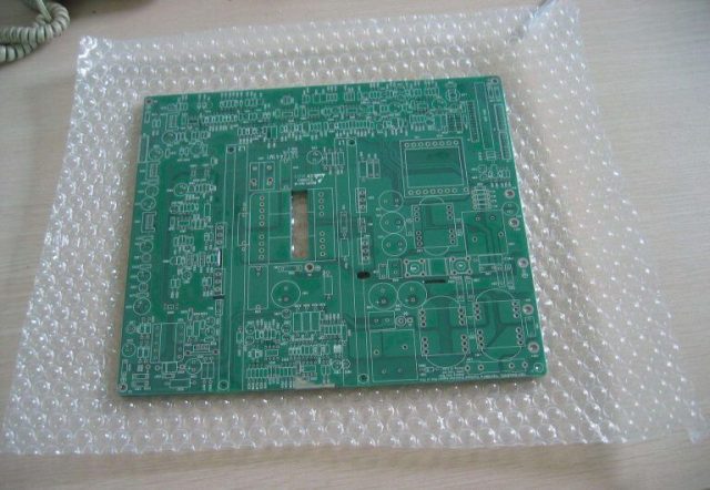
A Package Test PCB is a specialized semiconductor test PCB used to validate ICs after packaging and before final shipment. Installed in Automated Test Equipment (ATE) systems, the package test PCB serves as the electrical interface between the packaged device under test (DUT) and test instrumentation, enabling accurate functional, parametric, and reliability testing.
As semiconductor packaging technologies advance toward higher pin counts, finer pitch, and higher-speed interfaces, the performance requirements for package test PCBs continue to increase. A professionally engineered package test PCB ensures stable signal transmission, precise mechanical alignment, and repeatable test results across high-volume production environments.
Key Technical Requirements of Package Test PCBs
1. High Pin Count and High-Density Routing
Modern IC packages often include hundreds or thousands of I/O connections. Package test PCBs rely on HDI PCB technology to support fine-pitch fan-out and dense routing while maintaining signal integrity.
2. Controlled Impedance and Signal Integrity
High-speed digital and RF signals require precise controlled impedance routing. Optimized stackup design minimizes crosstalk, reflections, and signal loss during package-level testing.
3. Power Integrity and Low-Noise Design
Stable power delivery is essential for accurate IC testing. Multiple power and ground planes ensure low impedance paths and reduce voltage noise under dynamic test conditions.
4. Mechanical Accuracy and Socket Alignment
Package test PCBs must maintain tight mechanical tolerances to ensure proper alignment with test sockets and contactors, enabling consistent electrical contact over repeated test cycles.
5. Thermal Stability and Reliability
Package testing may involve high current or extended test times. Proper material selection and PCB construction ensure thermal stability and long-term reliability.
Applications of Package Test PCBs
Package test PCBs are widely used in:
-
Logic IC and processor package testing
-
Memory package testing for DRAM, NAND, and Flash
-
RF and mixed-signal IC package validation
-
Automotive-grade semiconductor testing
-
High-volume production and final test environments
Each application requires high accuracy, repeatability, and durability, making professional PCB manufacturing essential.
Manufacturing Capabilities for Package Test PCBs
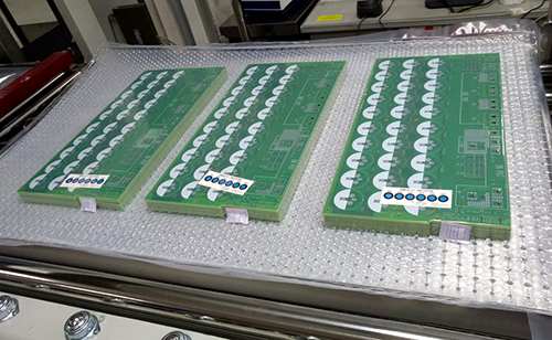
Producing a high-quality Package Test PCB requires advanced manufacturing capabilities, including:
-
HDI and multilayer PCB fabrication (12–30+ layers)
-
Controlled impedance measurement and verification
-
High-Tg and low-loss laminate options
-
Precision drilling and fine-line etching
-
Small batch prototyping and mass production support
These capabilities ensure consistent performance throughout the semiconductor test lifecycle.
Why Package Test PCB Quality Matters
Any variation in impedance, routing accuracy, or mechanical alignment can cause false test failures or yield loss. A high-quality package test PCB provides:
-
Accurate and repeatable test results
-
Reduced test downtime and debugging effort
-
Extended test socket and board lifespan
-
Improved semiconductor production yield
Conclusion
The Package Test PCB is a critical component in package-level semiconductor testing, enabling accurate validation of IC functionality, performance, and reliability. By combining HDI PCB technology, controlled impedance design, robust power integrity, and mechanical precision, package test PCBs support reliable testing across R&D and high-volume manufacturing.
Partnering with an experienced package test PCB manufacturer ensures consistent quality, faster validation cycles, and long-term semiconductor testing reliability.
