
Copper foil is one of the most fundamental materials in PCB manufacturing. Although it may appear to be a simple conductive layer, its properties directly influence signal integrity, insertion loss, thermal performance, reliability, and manufacturing quality.
As PCB technologies continue evolving toward:
- High-frequency RF applications
- High-speed digital systems
- Advanced automotive electronics
- 5G communication equipment
- Miniaturized electronic devices
the selection of suitable copper foil has become increasingly important.
Copper foil provides two essential functions in PCB structures:
- Electrical conduction for signal transmission and power distribution
- Thermal conduction for heat dissipation and temperature control
Beyond conductivity, characteristics such as copper type, surface roughness, treatment process, and crystal structure can significantly affect PCB performance.
Types of Copper Foil Used in PCB Manufacturing
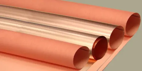
PCB copper foil is mainly divided into two categories:
- Rolled Annealed Copper (RA Copper)
- Electrodeposited Copper (ED Copper)
The two types have different manufacturing processes and performance characteristics, making them suitable for different PCB applications.
1. Rolled Annealed Copper (RA Copper)
RA copper foil is manufactured through a mechanical rolling process.
The production process begins with high-purity copper billets, which are repeatedly rolled and reduced until the required thickness is achieved.
This manufacturing method creates:
- A smooth copper surface
- A uniform crystal structure
- Excellent mechanical flexibility
Advantages of RA Copper
Due to its smooth surface profile, RA copper provides:
- Lower conductor loss
- Better high-frequency signal performance
- Improved flexibility for bending applications
Therefore, RA copper is commonly used in:
- Flexible PCBs
- Rigid-flex PCBs
- High-frequency RF circuits
- Ultra-high-speed digital applications
Limitations of RA Copper
Although RA copper offers excellent electrical performance, it also has some limitations:
- Higher material cost compared with ED copper
- More challenging fine-line etching capability
- Lower suitability for some high-volume rigid PCB applications
For applications where low insertion loss and mechanical flexibility are critical, RA copper remains an important material choice.
2. Electrodeposited Copper (ED Copper)
ED copper foil is produced through an electrochemical deposition process.
During manufacturing:
- Copper ions are dissolved in an electrolyte solution.
- A rotating titanium drum acts as the cathode.
- Copper gradually deposits onto the drum surface.
- The deposited copper layer is removed and processed into copper foil.
The rotation speed of the titanium drum affects:
- Copper thickness
- Crystal structure
- Surface characteristics
After production, ED copper foil typically undergoes additional surface treatments to improve bonding performance and oxidation resistance.
Copper Foil Surface Treatments
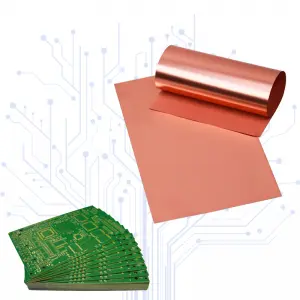
Copper foil requires different surface treatments depending on the PCB material system and application requirements.
These treatments serve several important purposes:
1. Improving Resin Adhesion
Different PCB laminate materials have different bonding characteristics.
Copper surface treatments help improve adhesion between copper foil and dielectric materials such as:
- FR-4
- PPE-based laminates
- PTFE materials
- High-frequency RF substrates
Proper copper treatment selection helps prevent:
- Layer separation
- Delamination
- Reliability failures during thermal cycling
2. Preventing Oxidation
Copper naturally oxidizes when exposed to air.
Surface protection treatments help:
- Reduce oxidation before PCB fabrication
- Maintain copper surface quality
- Improve long-term reliability
3. Enhancing High-Temperature Reliability
Certain copper treatments are designed to maintain stable bonding performance under:
- High operating temperatures
- Thermal cycling
- Long-term environmental stress
This is especially important for:
- Automotive electronics
- Industrial control systems
- High-power applications
Copper Foil Roughness and Its Impact on PCB Performance
Copper surface roughness is a critical parameter, especially for:
- RF PCB design
- Microwave circuits
- High-speed digital PCB applications
A rough copper surface improves mechanical bonding strength, but excessive roughness can increase signal loss.
At high frequencies, current flows mainly near the conductor surface due to the skin effect.
Therefore, increased copper roughness can cause:
- Higher conductor loss
- Increased insertion loss
- Signal phase variation
- Reduced transmission efficiency
For high-speed and high-frequency designs, engineers must balance:
- Adhesion reliability
- Electrical performance
Low Profile Copper Foil for High-Speed Applications
Electrodeposited copper foils are commonly classified according to surface roughness.
Industry classifications include:
- LP (Low Profile)
- VLP (Very Low Profile)
- HVLP (Hyper Very Low Profile)
Lower-profile copper foil provides:
- Reduced conductor loss
- Better signal transmission performance
- Improved high-frequency stability
These copper foils are widely applied in:
- 5G communication equipment
- High-speed servers
- Automotive radar systems
- Advanced computing platforms
Copper Foil Roughness Measurement Methods
Copper foil surface roughness can be measured using different techniques.
The two main approaches are:
1. Contact Measurement
Contact measurement uses a physical probe to scan the copper surface.
Advantages:
- Simple measurement method
- Widely used in traditional PCB manufacturing
Limitations:
- Limited accuracy for very small surface structures
- Probe size may affect measurement results
- Difficult to accurately capture narrow valleys
2. Non-Contact Measurement
Non-contact methods use technologies such as:
- Optical measurement
- Laser scanning
- White-light interferometry
Advantages:
- Higher measurement accuracy
- Better analysis of fine copper structures
- More suitable for advanced high-frequency applications
For RF and high-speed PCB analysis, non-contact measurement methods are generally preferred.
Copper Foil Roughness Parameters
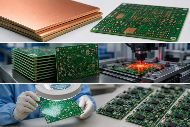
Different parameters are used to describe copper surface characteristics.
Rz (Peak-to-Valley Roughness)
Rz represents the height difference between the highest peak and lowest valley measured on the copper surface.
It is commonly used in PCB manufacturing evaluation.
Rq / Sq (Root Mean Square Roughness)
For high-frequency and high-speed digital designs, engineers often focus on:
- Rq
- Sq
These parameters better represent the electromagnetic influence of copper roughness.
Using electromagnetic modeling methods, Rq/Sq values can provide better correlation with actual circuit performance, including:
- Insertion loss
- Signal propagation delay
- Effective dielectric behavior
Surface Area Index (SAI)
Another important parameter is the Surface Area Index (SAI).
It represents the ratio between:
- Actual copper surface area including roughness
- Ideal flat surface area
SAI can be used in electromagnetic simulation models to improve prediction accuracy across wide frequency ranges.
Selecting the Right Copper Foil for PCB Applications
Different PCB applications require different copper foil characteristics.
| Application | Recommended Copper Considerations |
|---|---|
| Standard multilayer PCB | Standard ED copper |
| High-frequency RF PCB | Low-profile ED copper or RA copper |
| High-speed digital PCB | VLP/HVLP copper foil |
| Flexible PCB | RA copper |
| Automotive electronics | High-reliability treated copper |
| 5G and mmWave applications | Ultra-low roughness copper |
Proper copper foil selection helps achieve the required balance between:
- Electrical performance
- Mechanical reliability
- Manufacturing feasibility
- Cost efficiency
Conclusion
Copper foil selection is a critical factor in modern PCB engineering.
Beyond being a conductive layer, copper foil characteristics—including:
- Manufacturing process
- Surface treatment
- Roughness profile
- Crystal structure
- Mechanical properties
directly influence PCB reliability and signal performance.
For high-frequency, high-speed, and advanced electronic applications, engineers must carefully evaluate copper foil properties during the PCB material selection stage.
KKPCB provides comprehensive PCB and PCBA manufacturing services, including:
- PCB fabrication
- Prototype PCB production
- PCBA assembly
- SMT and DIP processing
- Functional testing
- Product assembly and packaging
With Gerber files or BOM information, KKPCB supports customers with reliable PCB and PCBA solutions tailored to different application requirements.
