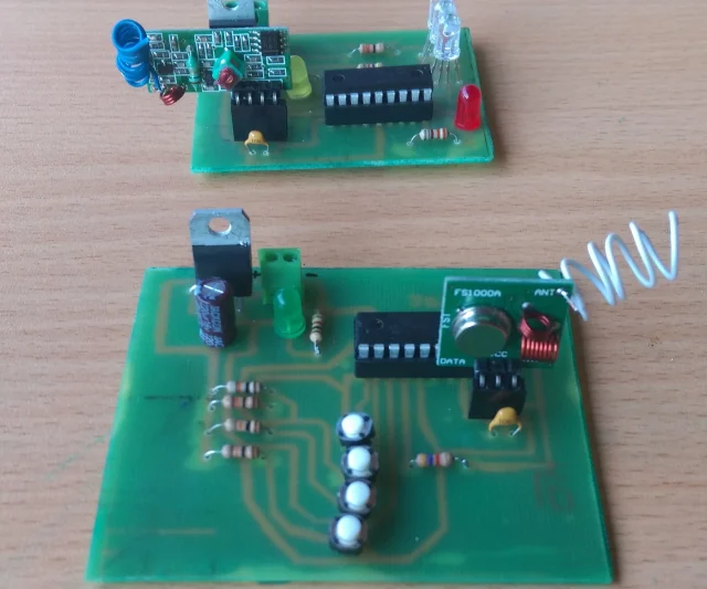
High-frequency communication systems—from 5G NR radios and phased-array front ends to satellite downlink modules and wideband radar—rely on precisely engineered RF Transceiver PCB architectures to maintain low-loss signal chains, stable phase performance, and strong EMI suppression. As operating frequencies rise into sub-6 GHz, C-band, Ku-band, Ka-band and even mmWave ranges, the electrical behavior of the RF Transceiver PCB becomes the defining factor that determines modulation accuracy, SNR performance, and link budget stability.
Designing a high-performance RF Transceiver PCB requires a coordinated engineering strategy across materials, stackups, routing structures, interconnect models, shielding techniques, and thermal control. The goal is simple: minimize loss, control electromagnetic behavior, and preserve clean, high-fidelity RF transmission through every stage of the transceiver chain.
1. Low-Loss PCB Materials Define RF Transceiver PCB High-Frequency Behavior
The first step to optimizing low-loss signal chains is selecting RF-grade laminates with predictable dielectric constants (Dk), ultra-low dissipation factors (Df), and minimal conductor surface roughness.
A high-frequency RF Transceiver PCB typically uses:
• PTFE-based laminates
• Low-Dk hydrocarbon ceramic composites
• Ultra-smooth rolled copper foils
• Temperature-stable dielectric systems for outdoor or aerospace operations
Low-loss materials reduce dielectric attenuation, control phase delay, and ensure that the RF Transceiver PCB maintains signal integrity across wide operating bandwidths.
2. Impedance-Controlled Stackups for Stable RF Transmission
In wideband RF transceivers, stable impedance is essential for consistent gain, linearity, and noise performance. The RF Transceiver PCB must be engineered with:
• Microstrip and grounded coplanar waveguide (GCPW) structures
• Stripline layers for LO, IF, or sensitive receive paths
• Tight dielectric thickness control
• Copper roughness modeling at high GHz frequencies
These controlled-impedance routing techniques prevent reflections, improve matching, and stabilize phase alignment across the entire RF signal chain.
3. HDI Architecture Enhances Compactness and Minimizes Parasitics
As RF communication modules become more compact, the RF Transceiver PCB must support dense routing without degrading signal quality.
Key HDI methods include:
• Laser-drilled microvias for RFIC breakout
• Via-in-pad structures to reduce inductive parasitics
• Stacked microvias for high-frequency vertical transitions
• Embedded passives for filter and matching networks
These structures minimize discontinuities, reduce current spreading, and maintain stable transmission performance even in ultra-compact PCB footprints.
4. EMI Control and RF Isolation for High-Density RF Modules
High-frequency transceiver chains generate—and are sensitive to—electromagnetic interference. EMI control is a core component of RF Transceiver PCB engineering.
Effective EMI strategies include:
• Stitching vias to create ground fencing
• Shielded cavities to isolate PA, LNA, LO, and synthesizer paths
• Segmented ground planes to prevent unwanted coupling
• RF absorbers or cavity structures in complex modules
Proper EMI control preserves modulation linearity, prevents intermodulation distortion, and ensures clean coexistence of multiple RF bands.
5. Thermal and Mechanical Stability for Long-Term Reliability
Power amplifiers, mixers, and broadband RF ICs generate significant heat. A robust RF Transceiver PCB must integrate:
• High-conductivity copper structures
• Thermal vias connecting to heat spreaders
• CTE-matched laminates for aerospace and outdoor systems
• Balanced stackups to minimize warpage
Maintaining thermal stability ensures reliable output power, stable phase performance, and long-term system integrity.
6. The Future of High-Frequency RF Transceiver PCB Design
As communication systems evolve toward higher frequencies, denser multi-band architectures, and more compact RF front ends, the RF Transceiver PCB becomes not just a carrier, but an active RF engineering platform. Future RF systems—from 6G THz links to advanced SATCOM payloads—will demand:
• Even lower-loss materials
• Hybrid stackups mixing RF, power, and digital domains
• AI-optimized routing and EM-driven layout
• Advanced shielding and isolation structures
The RF Transceiver PCB will remain the foundation for every next-generation wireless platform.
