
With the increasing demand for higher circuit density, faster signal transmission, and more complex electronic functions, multilayer printed circuit boards (PCBs) have become a fundamental technology in modern electronic products.
Unlike single-layer or double-sided PCBs, multilayer PCBs integrate multiple copper layers and insulating dielectric materials into one compact structure, allowing engineers to achieve complex routing, improved electrical performance, and better space utilization.
Multilayer PCBs are widely used in:
- Communication equipment
- Automotive electronics
- Industrial control systems
- Medical devices
- Semiconductor test equipment
- Aerospace electronics
- High-performance computing systems
The manufacturing process of multilayer PCBs involves multiple precision-controlled steps, including:
- Engineering review
- Material preparation
- Inner layer fabrication
- Layer lamination
- Drilling
- Copper plating
- Circuit pattern formation
- Surface finishing
- Inspection and testing
This article provides a complete overview of the multilayer PCB manufacturing process and explains the key considerations that influence PCB quality and reliability.
1. What Is a Multilayer PCB?
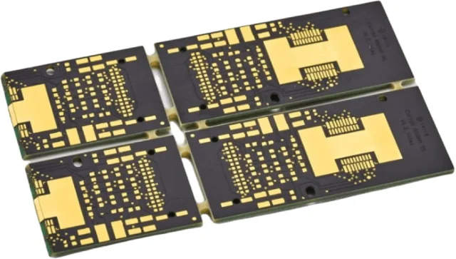
A multilayer PCB is a circuit board consisting of three or more conductive copper layers stacked together with insulating dielectric materials.
A typical multilayer PCB structure includes:
- Top copper layer
- Inner signal layers
- Ground planes
- Power planes
- Bottom copper layer
- Prepreg and core dielectric materials
Compared with traditional two-layer PCBs, multilayer boards provide:
Higher Wiring Density
Multiple internal layers allow more complex circuits to be routed within a limited space.
Better Signal Integrity
Dedicated ground and power planes help improve:
- Signal return paths
- Noise control
- Electromagnetic compatibility (EMC)
Improved Mechanical Reliability
The multilayer structure provides:
- Higher rigidity
- Better dimensional stability
- Stronger protection for internal circuits
2. Engineering Review and Manufacturing Preparation
Before production begins, PCB manufacturers perform a detailed engineering review.
The main purpose is to confirm:
- Manufacturing feasibility
- Electrical requirements
- Reliability risks
- Cost optimization
2.1 Design File Review
Manufacturers typically review:
- Gerber files
- Drill files
- PCB drawings
- BOM information (for PCBA projects)
- Stack-up requirements
Engineers evaluate:
- Trace width and spacing
- Via structures
- Layer arrangement
- Surface finish requirements
2.2 DFM (Design for Manufacturing) Analysis
DFM analysis helps identify potential production issues before fabrication.
Typical review items include:
- Minimum line width capability
- Via reliability
- Copper balance
- Hole-to-copper clearance
- Assembly requirements
Early DFM review can improve:
- Production yield
- Manufacturing efficiency
- Product reliability
3. Material Selection for Multilayer PCB
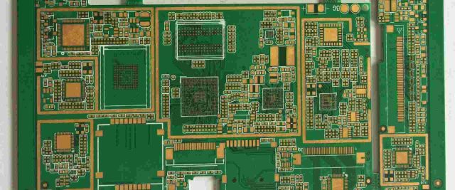
Material selection directly affects PCB performance.
Common materials include:
3.1 FR-4 Material
FR-4 is the most widely used PCB substrate.
Advantages:
- Good mechanical strength
- Stable electrical performance
- Cost-effective
Applications:
- Industrial electronics
- Consumer products
- General control boards
3.2 High-Tg FR-4 Material
High glass transition temperature (Tg) materials provide:
- Better thermal resistance
- Improved dimensional stability
Suitable for:
- Automotive electronics
- High-temperature environments
3.3 High-Frequency Materials
For high-speed and RF applications, specialized materials are required.
Examples:
- Rogers laminates
- PTFE materials
- Low-loss substrates
Important parameters:
- Dielectric constant (Dk)
- Dissipation factor (Df)
- Signal loss characteristics
Applications:
- RF circuits
- Microwave systems
- Radar electronics
4. Inner Layer Circuit Fabrication
The inner layer manufacturing process is one of the most important steps in multilayer PCB production.
4.1 Copper Foil Preparation
The process begins with:
- Core material preparation
- Copper foil cleaning
- Surface treatment
The copper surface must be clean to ensure proper adhesion.
4.2 Photoresist Coating
A photosensitive film is applied to the copper surface.
This layer protects areas that will become circuit patterns.
4.3 Exposure and Imaging
The circuit pattern is transferred onto the copper layer through exposure.
The process defines:
- Signal traces
- Pads
- Ground structures
High precision is required for:
- Fine-line circuits
- High-density designs
4.4 Etching Process
Unwanted copper is removed, leaving the required circuit pattern.
Process control affects:
- Trace width accuracy
- Signal performance
- Impedance consistency
4.5 Automated Optical Inspection (AOI)
AOI inspection verifies:
- Missing traces
- Short circuits
- Pattern defects
This prevents defective inner layers from entering later processes.
5. Layer Alignment and Lamination
After inner layer fabrication, multiple layers are stacked and laminated together.
5.1 Layer Stack-Up
The multilayer structure is arranged according to the PCB design.
A typical stack-up includes:
Important considerations:
- Signal layer arrangement
- Ground plane distribution
- Impedance requirements
5.2 Lamination Process
During lamination, heat and pressure bond all layers into a single PCB structure.
Key parameters include:
- Temperature
- Pressure
- Time
Proper lamination ensures:
- Strong layer bonding
- Stable electrical performance
- Mechanical reliability
5.3 Lamination Challenges
Incorrect lamination may cause:
- Delamination
- Layer shifting
- Resin voids
- Thickness variation
6. Drilling Process
After lamination, holes are drilled for electrical connections.
Drilling methods include:
Mechanical Drilling
Used for:
- Through holes
- Larger vias
Laser Drilling
Used for:
- Microvias
- HDI structures
Advantages:
- Higher precision
- Smaller hole size
Controlled Depth Drilling
Used when specific layer connections are required.
Applications:
- High-speed PCBs
- Advanced multilayer designs
7. Copper Plating Process
After drilling, the hole walls must become conductive.
The process includes:
7.1 Electroless Copper Deposition
A thin copper layer is deposited on:
- Hole walls
- PCB surfaces
This creates initial electrical conductivity.
7.2 Electrolytic Copper Plating
Additional copper is plated to achieve required thickness.
This ensures:
- Reliable via connections
- Mechanical strength
Poor plating quality may cause:
- Via cracks
- Open circuits
8. Outer Layer Circuit Formation
The outer circuit pattern is created using similar processes as inner layers.
Steps include:
- Photo imaging
- Copper plating
- Etching
- Inspection
The outer layers contain:
- Component pads
- Connection points
- External routing
9. Solder Mask Application
Solder mask is applied to protect copper surfaces.
Functions include:
- Prevent solder bridging
- Protect circuits from oxidation
- Improve insulation reliability
Common solder mask colors include:
- Green
- Blue
- Black
- Red
10. Surface Finish Application
Surface finishing improves:
- Solderability
- Corrosion resistance
- Component assembly reliability
Common finishes include:
ENIG
Advantages:
- Flat surface
- Suitable for fine-pitch components
Applications:
- SMT assembly
- BGA components
ENEPIG
Advantages:
- Higher reliability
- Suitable for advanced applications
Applications:
- Semiconductor products
- High-reliability electronics
HASL
Advantages:
- Cost-effective
- Good solderability
11. PCB Electrical Testing
Electrical testing verifies circuit continuity and isolation.
Common methods include:
Flying Probe Testing
Suitable for:
- Prototypes
- Small batches
Fixture Testing
Suitable for:
- Mass production
Tests:
- Open circuits
- Short circuits
- Electrical connections
12. Quality Inspection and Reliability Testing
Multilayer PCBs require strict quality control.
Common inspection methods include:
AOI Inspection
Detects:
- Circuit defects
- Pattern abnormalities
X-Ray Inspection
Used for:
- Internal structures
- Hidden defects
Microsection Analysis
Evaluates:
- Copper thickness
- Via quality
- Layer bonding
Reliability Testing
May include:
- Thermal cycling
- Humidity testing
- Mechanical stress testing
13. Key Manufacturing Challenges of Multilayer PCBs
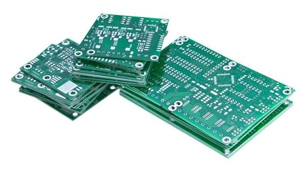
13.1 Layer Alignment Accuracy
More layers increase alignment difficulty.
Poor registration may cause:
- Via connection problems
- Signal performance issues
13.2 Impedance Control
High-speed multilayer PCBs require precise control of:
- Trace width
- Dielectric thickness
- Material properties
13.3 Thermal Management
Complex multilayer designs require consideration of:
- Heat distribution
- Copper plane design
- Thermal vias
13.4 Manufacturing Yield
Higher layer counts increase:
- Process complexity
- Inspection requirements
- Production risks
14. Applications of Multilayer PCBs
Communication Equipment
Applications:
- Network devices
- Base stations
- RF systems
Requirements:
- High-speed transmission
- Signal integrity
Automotive Electronics
Applications:
- Vehicle controllers
- ADAS systems
- Sensor modules
Requirements:
- Reliability
- Temperature resistance
Industrial Control Systems
Applications:
- Automation equipment
- Control boards
Requirements:
- Long-term stability
Semiconductor Equipment
Applications:
- ATE load boards
- Test interface boards
Requirements:
- High-density routing
- Precise electrical performance
Conclusion
The multilayer PCB manufacturing process combines advanced engineering design, precision fabrication, and strict quality control.
From:
- Material selection
- Inner layer fabrication
- Lamination
- Drilling
- Copper plating
- Surface finishing
- Electrical testing
each manufacturing stage directly affects PCB performance and reliability.
As electronic products continue evolving toward higher speed, smaller size, and greater integration, multilayer PCB technology will remain a critical foundation supporting modern electronic innovation.
