What Is a Multilayer HF PCB?
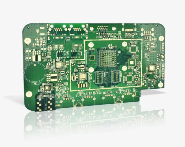
A Multilayer HF PCB (High Frequency PCB) is a multilayer printed circuit board designed to support high-frequency signal transmission, typically in the MHz to GHz range.
Unlike single or double-layer RF boards, multilayer HF PCBs integrate multiple signal layers, ground planes, and power planes within a compact stack-up. This allows complex RF routing, shielding, and controlled impedance structures to coexist in one design.
They are widely used in advanced communication, radar, and wireless systems.
Why Multilayer Structure Matters in HF Design
As system complexity increases, high-frequency circuits require:
-
Multiple RF channels
-
Dense signal routing
-
Dedicated grounding layers
-
Integrated power distribution
-
Mixed digital and RF sections
A multilayer structure enables:
-
Improved signal isolation
-
Reduced electromagnetic interference (EMI)
-
Stable return paths
-
Compact layout integration
Proper stack-up design is critical for RF stability.
Key Design Requirements
1. Controlled Impedance Across Layers
High-frequency signals demand precise impedance control. Multilayer HF PCBs must:
-
Maintain consistent dielectric thickness
-
Use stable Dk materials
-
Ensure accurate trace width calculation
-
Control manufacturing tolerances
Impedance variation directly affects signal reflection and insertion loss.
2. Low Loss Materials Selection
HF multilayer boards often use low-loss laminates provided by companies such as:
-
Rogers Corporation
-
Taconic
These materials offer:
-
Low dissipation factor (Df)
-
Stable dielectric constant (Dk)
-
High-frequency reliability
In some cases, hybrid stack-ups combine low-loss material for RF layers and FR4 for non-critical layers to optimize cost.
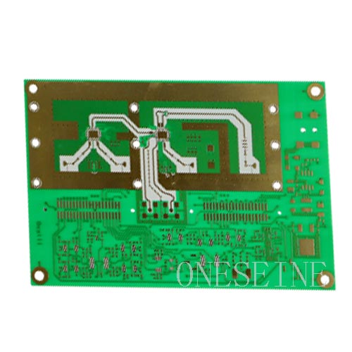
3. Grounding and Isolation
Multilayer HF PCB design typically includes:
-
Dedicated ground planes between RF layers
-
Via fences for signal shielding
-
Short return paths
-
Segregation of analog, RF, and digital sections
Effective grounding minimizes cross-talk and radiation.
4. Via Optimization
High-frequency performance can degrade due to via stubs and parasitic effects.
Common techniques include:
-
Back-drilling
-
Blind or buried vias
-
Microvia structures
-
Short via transitions
Proper via design reduces signal reflection and improves bandwidth performance.
5. Thermal Stability
In RF power systems, heat may affect dielectric performance. Multilayer HF PCBs must maintain:
-
Dimensional stability
-
Low CTE mismatch
-
Reliable plating integrity
Thermal control ensures consistent RF characteristics.
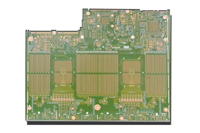
Typical Layer Configurations
Multilayer HF PCBs are commonly built as:
-
4-layer RF stack-ups
-
6-layer communication boards
-
8-layer radar modules
-
Mixed digital + RF integration boards
Layer planning balances signal integrity, shielding, and mechanical strength.
Applications of Multilayer HF PCB
Multilayer HF PCBs are widely used in:
-
5G base station equipment
-
Microwave communication modules
-
Radar systems
-
Satellite communication devices
-
RF transceiver boards
-
Aerospace communication systems
As frequency increases, multilayer integration becomes essential.
Multilayer HF PCB vs Standard Multilayer PCB
| Feature | Standard Multilayer PCB | Multilayer HF PCB |
|---|---|---|
| Frequency Range | Low to Medium | High (GHz range) |
| Material Type | FR4 | Low Loss HF Materials |
| Impedance Accuracy | Moderate | High |
| EMI Control | Basic | Advanced |
| Cost | Lower | Higher |
Multilayer HF PCB focuses on electrical precision rather than only structural integration.
Conclusion
Multilayer HF PCB technology enables complex high-frequency system integration while maintaining signal stability and minimal loss. Through advanced stack-up design, low-loss material selection, and optimized grounding strategies, these PCBs support reliable performance in RF and microwave applications.
For modern communication and radar systems, multilayer HF PCB design is a critical foundation for achieving stable, high-bandwidth signal transmission.
