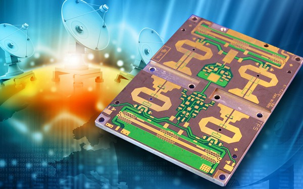
A Microwave IC Test PCB is a specialized semiconductor test PCB designed for testing integrated circuits operating in the microwave and millimeter-wave frequency ranges, typically from several GHz up to tens of GHz. These PCBs are widely used in Automated Test Equipment (ATE) systems to characterize critical microwave parameters such as gain, insertion loss, phase stability, isolation, and linearity.
As microwave ICs are increasingly applied in 5G mmWave communication, automotive radar, satellite systems, and advanced RF front-end modules, the performance of the microwave IC test PCB directly impacts measurement accuracy and test repeatability.
Key Design Characteristics of Microwave IC Test PCBs
1. Ultra-Low Loss Material Selection
Microwave IC test PCBs require low dielectric constant (Dk) and low dissipation factor (Df) materials to minimize signal attenuation and phase distortion at high frequencies. Proper material selection ensures stable performance across GHz and mmWave bands.
2. Precise Controlled Impedance Routing
Maintaining strict controlled impedance is essential for microwave signal integrity. Trace geometry, dielectric thickness, and reference planes must be carefully designed to reduce reflection, return loss, and impedance discontinuities.
3. Superior Signal Integrity at High Frequencies
Microwave IC test PCBs must control EMI, crosstalk, parasitic effects, and radiation loss. Short signal paths, optimized ground structures, and isolation techniques are critical for clean microwave measurements.
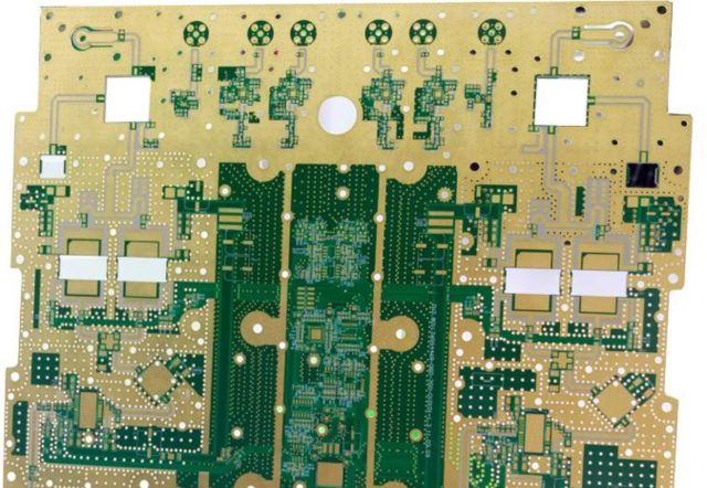
4. High-Density Interconnect and Fine Pitch Layouts
Many microwave ICs integrate RF, analog, and digital functions in compact packages. HDI PCB technology, microvias, and fine-line routing enable dense interconnects without compromising microwave performance.
5. Mechanical Accuracy and RF Interface Stability
Precise pad alignment, excellent PCB flatness, and stable mechanical construction ensure reliable contact with RF probes, coaxial connectors, and test sockets, especially during repeated test cycles.
Applications of Microwave IC Test PCBs
Microwave IC test PCBs are commonly used in:
-
5G mmWave IC and module testing
-
Automotive radar and ADAS semiconductor validation
-
Satellite and aerospace microwave IC testing
-
High-frequency RF front-end module evaluation
-
Wireless infrastructure and base station IC testing
These applications demand extremely low signal loss and high measurement accuracy.
Manufacturing Requirements for Microwave IC Test PCBs
Producing high-performance microwave IC test PCBs requires advanced manufacturing processes, including:
-
Controlled impedance multilayer fabrication
-
Low-loss laminate processing
-
Precision drilling and via control
-
Fine-line and HDI manufacturing
-
Impedance testing and RF performance verification
Manufacturing precision ensures repeatable electrical performance and long-term reliability.
Why Microwave IC Test PCB Quality Is Critical
Inferior microwave IC test PCBs can cause:
-
Excessive insertion loss and signal distortion
-
Measurement inconsistency and inaccurate RF data
-
Increased noise, EMI, and parasitic effects
-
Reduced ATE efficiency and lower test yield
A high-quality microwave IC test PCB ensures accurate high-frequency characterization and stable test results across demanding microwave applications.
Conclusion
The Microwave IC Test PCB is a key enabler for high-frequency and mmWave semiconductor testing, delivering controlled impedance, ultra-low loss performance, and mechanical precision. By combining advanced materials, HDI layout techniques, and precision manufacturing, microwave IC test PCBs support accurate, repeatable testing for next-generation communication, radar, and satellite systems.
Partnering with an experienced microwave IC test PCB manufacturer helps ensure measurement accuracy, testing efficiency, and long-term reliability for high-frequency semiconductor validation.
