What Is a Microvia PCB
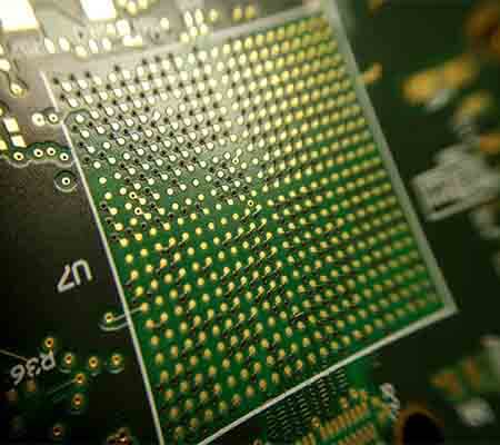
A Microvia PCB is a high-density interconnect (HDI) printed circuit board that uses laser-drilled microvias to connect adjacent copper layers. Unlike traditional mechanical through-holes, microvias are extremely small and typically connect only one or two layers.
Microvia technology enables higher routing density, improved electrical performance, and more compact electronic designs.
What Is a Microvia?
A microvia is defined by its small diameter, typically:
-
Diameter: ≤ 150 µm
-
Laser-drilled instead of mechanically drilled
-
Used for layer-to-layer interconnection
-
Commonly applied in HDI stack-up structures
Microvias allow vertical interconnections without occupying excessive routing space.
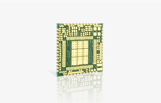
Types of Microvia Structures
1. Stacked Microvia
Microvias are vertically aligned on top of each other, enabling multiple layer transitions in compact areas.
Used in high-density BGA designs and advanced processor boards.
2. Staggered Microvia
Microvias are offset rather than stacked directly.
Provides improved reliability and reduced stress concentration.
3. Via-in-Pad
Microvias are placed directly inside component pads, maximizing routing space under fine-pitch BGA components.
Why Microvia PCB Is Important
Modern electronics require:
-
Smaller board size
-
Higher component density
-
Increased signal layers
-
Better signal integrity
Microvia PCB enables:
-
Efficient escape routing for fine-pitch components
-
Reduced layer count in some designs
-
Shorter signal paths
-
Lower parasitic inductance
This improves overall electrical performance and compactness.
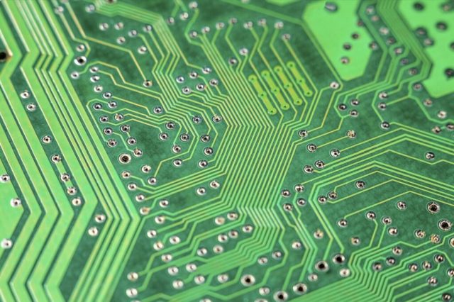
Manufacturing Process of Microvia PCB
Producing microvias requires advanced fabrication technology:
1. Laser Drilling
High-precision laser systems create small-diameter vias with controlled depth.
2. Sequential Lamination
Multiple lamination cycles allow layer build-up structures for HDI boards.
3. Via Filling and Plating
Microvias are copper-filled or plated to ensure structural stability and electrical conductivity.
4. Precision Imaging
Laser Direct Imaging (LDI) ensures accurate alignment between layers.
Electrical and Mechanical Advantages
Microvia PCB offers:
-
Shorter interconnection paths
-
Reduced signal reflection
-
Lower via stub effect
-
Improved high-speed performance
-
Enhanced reliability under thermal cycling
Proper design ensures strong copper filling and long-term reliability.
Applications of Microvia PCB
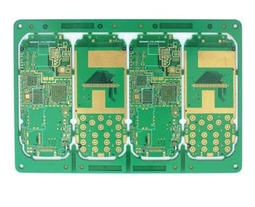
Microvia PCBs are widely used in:
-
Smartphones and tablets
-
High-performance computing modules
-
AI accelerator boards
-
Networking and data center equipment
-
Automotive ADAS systems
-
Medical electronic devices
-
Aerospace control electronics
As devices continue to shrink and increase in complexity, microvia technology becomes essential.
Microvia PCB vs Through-Hole PCB
| Feature | Through-Hole PCB | Microvia PCB |
|---|---|---|
| Via Size | Larger | Very Small |
| Layer Connection | All layers | Adjacent layers |
| Routing Density | Moderate | High |
| Signal Performance | Standard | Improved |
| Manufacturing Complexity | Lower | Higher |
Microvia PCB supports advanced HDI designs with significantly higher interconnection density.
Conclusion
Microvia PCB technology is a cornerstone of modern HDI design. By enabling laser-drilled, high-density vertical interconnections, it supports compact layouts, improved signal integrity, and advanced multilayer architectures.
For high-speed, high-density electronic systems requiring miniaturization and performance optimization, microvia PCB remains a critical manufacturing solution.
