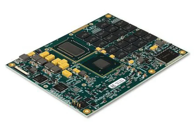
In modern electronics, especially in RF, 5G, and high-speed communication systems, signal loss can significantly affect device performance. Low loss PCBs are specifically designed to minimize dielectric and conductor losses, ensuring high-frequency signals propagate with minimal attenuation. These PCBs are essential for applications such as mmWave modules, RF transceivers, antennas, and satellite communication systems.
Design Considerations
-
Controlled Impedance:
High-frequency signals require consistent impedance across all traces to prevent reflections, standing waves, or signal degradation. Designers must carefully select trace width, spacing, and layer stack-up, while maintaining proper grounding and shielding to optimize signal integrity. -
Minimizing Crosstalk and Noise:
Low loss PCBs often include solid ground planes, shielding strategies, and proper layer separation to reduce electromagnetic interference (EMI) and crosstalk. Differential pair routing is commonly employed for high-speed signals to maintain signal fidelity. -
Stack-Up Optimization:
The choice of layer stack-up impacts dielectric losses, thermal management, and mechanical stability. HDI techniques and microvia placement can further improve routing density while maintaining low loss performance.
Material Selection
The core of low loss PCB performance lies in the dielectric material:
-
Low Dielectric Constant (Dk): Reduces signal propagation delay and maintains consistent impedance.
-
Low Dissipation Factor (Df): Minimizes energy loss during signal transmission.
-
High Thermal Stability: Materials like Rogers laminates, PTFE composites, and high-performance FR-4 variants withstand thermal cycles without warping, maintaining performance over time.
Manufacturing Considerations
Producing low loss PCBs requires precise fabrication techniques:
-
Controlled Etching: Ensures accurate trace dimensions and spacing to maintain impedance.
-
Plating and Copper Thickness Management: Optimizes conductor losses and signal propagation.
-
Lamination and Layer Alignment: High-frequency performance is sensitive to layer misalignment; sequential lamination ensures reliable multilayer boards.
KKPCB applies advanced process control and high-precision manufacturing to deliver low loss PCBs with consistent electrical characteristics and high reliability.
Testing and Quality Assurance
Low loss PCBs undergo rigorous validation to ensure performance:
-
Impedance Testing: Verifies controlled impedance and differential pair consistency.
-
Time Domain Reflectometry (TDR): Detects impedance discontinuities along high-speed traces.
-
High-Frequency Signal Testing: Confirms signal attenuation, crosstalk, and insertion loss meet design specifications.
-
AOI and X-ray Inspection: Checks surface and internal defects, including via integrity and layer alignment.
Applications of Low Loss PCBs
Low loss PCBs are critical in industries that require high-frequency performance and minimal signal degradation:
-
5G and Next-Generation Networking: Ensuring reliable signal propagation in mmWave modules and antennas.
-
RF and Microwave Devices: Low loss materials reduce insertion loss for transceivers, filters, and amplifiers.
-
Satellite Communication Systems: Maintaining signal fidelity across long transmission paths.
-
High-Speed Computing and Data Centers: Supporting high-speed interconnects and signal-intensive processing boards.
By combining careful design, advanced materials, precise manufacturing, and rigorous testing, KKPCB delivers low loss PCBs capable of meeting the demanding requirements of modern high-frequency electronics.
