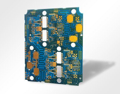
As modern electronic systems operate at increasingly higher frequencies and faster data rates, signal loss has become a major challenge in PCB design. Low Loss PCBs are specifically engineered to minimize signal attenuation and maintain signal integrity in high-speed and high-frequency circuits.
Unlike conventional FR-4 boards, low loss PCBs use advanced dielectric materials with lower dissipation factors, enabling efficient signal transmission with minimal distortion. These PCBs are widely used in applications such as 5G communication systems, high-speed networking equipment, radar systems, aerospace electronics, and advanced computing hardware.
By reducing dielectric and conductor losses, low loss PCBs help ensure reliable performance in demanding electronic environments.
What Is a Low Loss PCB?
A Low Loss PCB is a printed circuit board manufactured using specialized dielectric materials designed to reduce signal attenuation at high frequencies. Signal loss typically occurs due to dielectric loss within the substrate and conductor loss along the copper traces.
Low loss materials have a low dissipation factor (Df) and stable dielectric constant (Dk), which help maintain signal quality across long trace lengths and high-frequency transmissions.
These boards are particularly important in systems operating in the GHz range, where even small losses can significantly affect signal performance.
Key Characteristics of Low Loss PCBs
Low Dissipation Factor (Df)
Low loss PCB materials exhibit a very small dissipation factor, reducing energy loss as signals propagate through the board.
Stable Dielectric Constant (Dk)
A stable dielectric constant ensures consistent impedance control and predictable signal behavior.
High Signal Integrity
Low loss substrates help reduce signal distortion, jitter, and attenuation in high-speed circuits.
Improved Thermal Stability
Many low loss materials offer excellent thermal performance, making them suitable for high-power and high-frequency applications.
Common Materials Used in Low Loss PCBs
Several high-performance materials are commonly used to manufacture low loss PCBs:
-
PTFE-based laminates
-
Rogers high-frequency materials
-
Low-loss hydrocarbon ceramic laminates
-
Advanced high-speed digital materials
These materials provide improved electrical properties compared to traditional FR-4 substrates, especially at high frequencies.
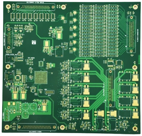
Applications of Low Loss PCBs
Low loss PCBs are widely used in advanced electronic systems where signal performance is critical.
5G Communication Equipment
Base stations, antennas, and RF modules require low loss PCBs to support high-frequency signal transmission.
High-Speed Data Networks
Servers, routers, and high-speed switches rely on low loss boards to maintain signal integrity across high-speed data channels.
Radar and Aerospace Systems
Low loss PCBs enable precise signal transmission in radar systems and satellite communication equipment.
Automotive Radar and ADAS
Modern vehicles incorporate radar sensors and communication systems that operate at high frequencies.
High-Performance Computing
Low loss PCBs are used in data centers and AI computing platforms to support high-speed processing architectures.
Design Considerations for Low Loss PCBs
Designing low loss PCBs requires careful attention to several factors.
Material Selection
Choosing the correct dielectric material with low Df and stable Dk is essential for maintaining signal quality.
Controlled Impedance Routing
Precise impedance control is required for high-speed differential pairs and RF transmission lines.
Trace Geometry Optimization
Wider traces, smoother copper surfaces, and optimized routing paths help reduce conductor loss.
Stackup Design
Proper layer stackup and ground plane placement minimize signal interference and maintain return paths.
Conclusion
Low loss PCBs play an essential role in supporting modern high-frequency and high-speed electronic systems. By using advanced materials and optimized PCB design techniques, engineers can significantly reduce signal attenuation and maintain excellent signal integrity.
As technologies such as 5G networks, high-speed computing, satellite communication, and advanced radar systems continue to develop, the demand for reliable low loss PCB solutions will continue to grow.
