What Is a Load Board PCB?
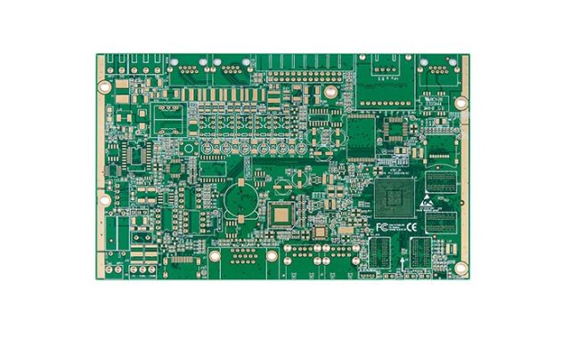
A Load Board PCB is a critical interface board used in Automated Test Equipment (ATE) systems for semiconductor device testing. It connects the tester to the device under test (DUT), transmitting signals, power, and measurement data with high accuracy and stability.
Load boards are specifically engineered to support high pin count devices, high-speed signals, and precise electrical measurement environments. Their performance directly affects test accuracy, repeatability, and production yield.
Key Functions of a Load Board PCB
Load board PCBs are designed to:
-
Route test signals between ATE system and DUT
-
Provide stable and low-noise power delivery
-
Support high-speed and high-frequency interfaces
-
Maintain mechanical alignment with test sockets
-
Ensure repeatable electrical performance
As semiconductor devices become more complex, load boards must handle increasing data rates and tighter tolerances.
Technical Requirements of Load Board PCB
1. High Layer Count Structure
Modern load boards often require:
-
10–30+ layer multilayer design
-
Dedicated ground and power planes
-
Controlled signal layer separation
High layer count enables dense routing and stable signal reference.
2. Controlled Impedance and Signal Integrity
High-speed interfaces such as DDR, PCIe, SerDes, and RF signals require:
-
Strict impedance control
-
Differential pair matching
-
Reduced via stubs (back drilling)
-
Low loss laminate materials
Stable impedance ensures accurate timing and signal measurement.
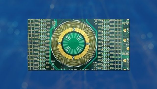
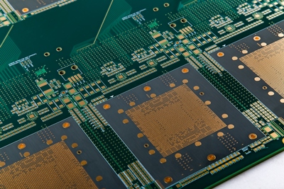
3. HDI and Fine Pitch Capability
Load boards frequently support:
-
Fine pitch BGA packages
-
Microvia structures
-
Blind and buried vias
-
Via-in-pad technology
High-density interconnect technology allows routing of high pin count devices in compact layouts.
4. Mechanical Precision and Flatness
Precise alignment between DUT and socket is essential. Load board PCB must maintain:
-
Tight dimensional tolerance
-
Minimal warpage
-
Consistent thickness control
Mechanical stability ensures reliable contact and reduces test variation.
5. Thermal and Current Handling
Certain test conditions require:
-
Heavy copper layers
-
Stable thermal management
-
High TG materials
-
Reinforced power planes
This ensures reliability during continuous test cycles.
Applications of Load Board PCB
Load board PCBs are widely used in:
-
IC package testing
-
Wafer probe interface systems
-
Automotive semiconductor validation
-
RF device testing
-
Memory and processor testing
-
High-speed communication chip validation
As chips move toward higher frequencies and higher pin density, load board complexity continues to increase.
Load Board PCB vs Standard PCB
| Feature | Standard PCB | Load Board PCB |
|---|---|---|
| Purpose | General Electronics | Semiconductor Testing |
| Layer Count | Moderate | High |
| Impedance Control | Optional | Strict |
| Mechanical Tolerance | Standard | Tight |
| Reliability Requirement | Normal | Critical |
Load board PCBs are engineered specifically for precision measurement and high test repeatability.
Manufacturing Capabilities
Professional load board PCB fabrication may include:
-
12–30+ layer construction
-
HDI microvia processing
-
Back drilling
-
Controlled impedance verification
-
Low loss and high TG materials
-
X-ray and AOI inspection
-
100% electrical testing
Strong process control ensures stable performance across high-volume test cycles.
Conclusion
Load Board PCB is a core component in semiconductor testing systems. With high layer count architecture, precise impedance control, and advanced HDI technology, load boards enable accurate and reliable device validation.
As semiconductor devices continue to evolve toward higher speed and complexity, advanced load board PCB solutions remain essential for maintaining test accuracy and manufacturing yield.
