What Is a Load Board PCB?
A Load Board PCB is a critical component used in Automated Test Equipment (ATE) systems for semiconductor device testing. It provides the electrical interface between the ATE tester and the device under test (DUT), enabling accurate signal transmission, power delivery, and measurement.
Load Board PCB is commonly used in:
-
Final package testing
-
Wafer level testing
-
Memory device testing
-
Logic IC validation
-
RF and high speed chip testing
In modern semiconductor manufacturing, Load Board PCB ensures that integrated circuits meet electrical performance and reliability standards before shipment.
Key Functions of Load Board PCB
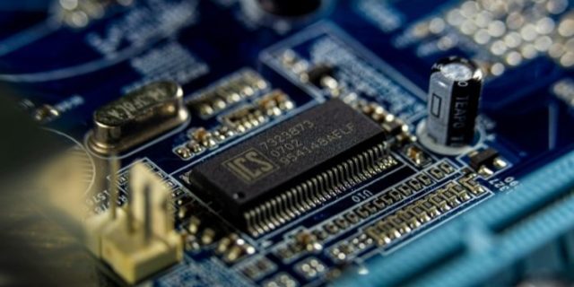
1. Signal Routing and High Speed Transmission
Load Board PCB must handle:
-
High speed digital signals
-
Differential pair routing
-
RF signal paths
-
Low skew timing control
Controlled impedance design ensures minimal reflection and stable high bandwidth communication.
2. Power Delivery and Current Handling
Load Board PCB distributes multiple voltage domains to the DUT. It must support:
-
Low impedance power planes
-
High current traces
-
Stable grounding structure
Stable power distribution is essential for accurate electrical characterization.
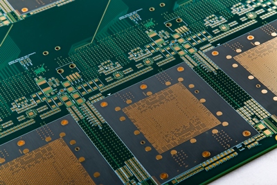
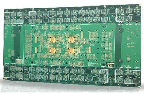
3. High Pin Count and Fine Pitch Support
Modern semiconductor packages often include:
-
BGA and LGA packages
-
Fine pitch ball grids
-
Thousands of I/O pins
Load Board PCB uses advanced routing technologies such as:
-
HDI structures
-
Blind and buried vias
-
Back drilling
-
Sequential lamination
These technologies enable efficient routing within limited board space.
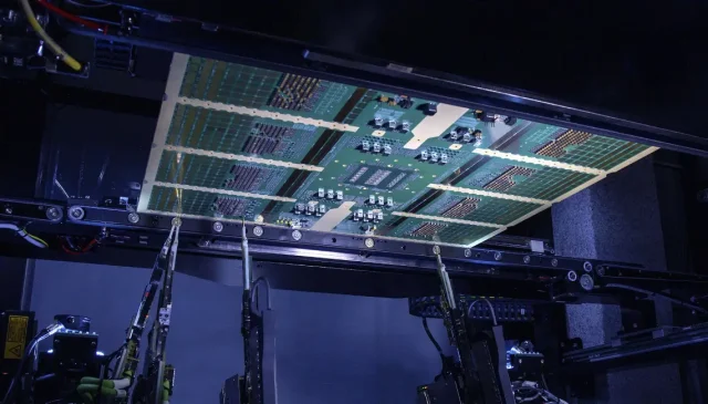
4. Mechanical and Thermal Reliability
Load Board PCB must withstand:
-
Repeated socket insertion cycles
-
High temperature burn-in conditions
-
Long test durations
High TG materials and stable laminate structures improve durability and long-term performance.
Technical Capabilities of Load Board PCB
Load Board PCB manufacturing may include:
-
8–40+ layer multilayer structures
-
Controlled impedance (50Ω / 100Ω differential)
-
Low loss materials for high frequency testing
-
Heavy copper for power semiconductor testing
-
Fine line processing for dense routing
-
Via-in-pad technology
-
Impedance testing and electrical verification
Strict manufacturing tolerance ensures repeatable test accuracy.
Applications of Load Board PCB
Load Board PCB is widely used in:
-
Logic IC testing
-
Memory testing (DDR, NAND, NOR)
-
RF IC validation
-
Automotive chip qualification
-
Power device testing
-
5G communication chip evaluation
As semiconductor devices increase in speed and complexity, Load Board PCB design requirements continue to grow.
Load Board PCB vs Standard PCB
| Feature | Load Board PCB | Standard PCB |
|---|---|---|
| Application | Semiconductor Testing | Consumer Electronics |
| Pin Density | Very High | Moderate |
| Signal Speed | High / Ultra High | Standard |
| Impedance Control | Strict | Optional |
| Reliability Requirement | Critical | Normal |
Load Board PCB is engineered specifically for high accuracy, repeatability, and stability in test environments.
Conclusion
Load Board PCB is a key infrastructure component in semiconductor testing. It ensures accurate signal transmission, stable power delivery, and reliable DUT evaluation in ATE systems.
With increasing data rates and higher pin density devices, selecting an experienced Load Board PCB manufacturer is essential for achieving precision, durability, and long-term reliability.
