
The Role of Load Board PCB in Semiconductor Testing
In semiconductor manufacturing, test accuracy, production efficiency, and overall yield are critical factors affecting product cost and reliability. As the electrical interface between Automated Test Equipment (ATE) and the Device Under Test (DUT), the load board PCB plays a key role in ensuring accurate and repeatable semiconductor testing.
Unlike conventional PCBs used in electronic products, load board PCBs are specifically designed for high-frequency signals, high pin-count connections, continuous testing cycles, and strict electrical performance requirements.
A reliable load board PCB must maintain stable signal transmission, consistent power delivery, and mechanical reliability throughout thousands or even millions of test cycles.
What Makes Load Board PCB Different from Conventional PCBs?
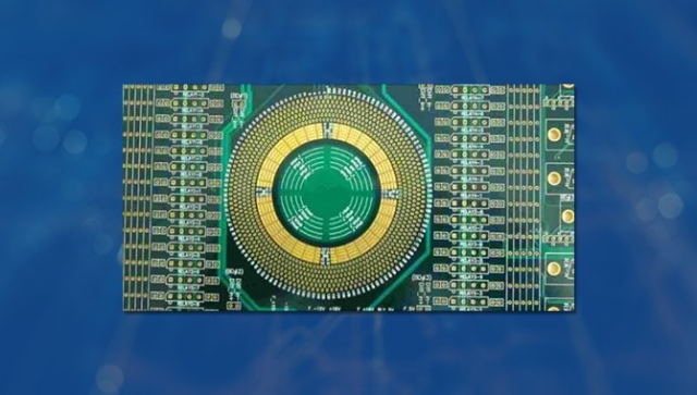
A load board PCB is a specialized test interface board used in semiconductor final testing and validation. It connects the ATE system with packaged IC devices through sockets, connectors, or custom test fixtures.
Compared with standard functional PCBs, load board PCBs focus more on:
- Electrical performance consistency rather than product functionality
- High-density signal interconnection
- Precise impedance control
- Long-term mechanical durability
- Repeatable testing performance
Any variation in PCB performance can directly influence test accuracy, false failure rates, and semiconductor production yield.
Key Design Challenges in Load Board PCB Development
1. Signal Integrity and High-Speed Performance
Modern semiconductor devices operate with higher data rates and tighter electrical margins. During testing, even small signal distortions can affect measurement accuracy.
Common signal integrity challenges include:
- Impedance variation
- Signal loss
- Crosstalk
- Timing skew
- High-frequency transmission instability
To address these challenges, load board PCB design typically requires:
- Controlled impedance routing
- Optimized stack-up design
- Short and balanced signal paths
- Proper reference plane configuration
- High-frequency material selection
Maintaining consistent signal behavior helps ensure reliable IC test results and reduces measurement errors.
2. Power Delivery Stability Under Dynamic Loads
Load board PCBs often supply power directly to semiconductor devices during testing. Fluctuations in power delivery can lead to unstable test conditions or inaccurate results.
Important design considerations include:
- Low-impedance power distribution networks
- Sufficient copper thickness
- Optimized power and ground planes
- Effective decoupling capacitor placement
- Current carrying capability analysis
A well-designed power delivery network helps maintain voltage stability during dynamic testing conditions.
3. Thermal Management and Mechanical Reliability
Semiconductor testing environments often involve continuous operation, repeated thermal cycling, and mechanical stress from socket connections.
Key reliability considerations include:
- PCB flatness control
- Connector and socket area reinforcement
- Material thermal stability
- Layer structure optimization
- Warpage prevention
Mechanical consistency is essential because even minor deformation may affect socket contact reliability and test repeatability.
4. PCB Manufacturing Precision and Process Control
The performance of a load board PCB depends not only on design but also on manufacturing consistency.
Critical manufacturing requirements include:
- Accurate layer registration
- Stable dielectric thickness
- Uniform copper distribution
- Reliable via plating
- Controlled impedance fabrication
- Tight dimensional tolerances
For semiconductor test applications, manufacturing variation must be minimized to ensure consistent performance between prototype builds and production quantities.
Material Selection for Load Board PCB Applications
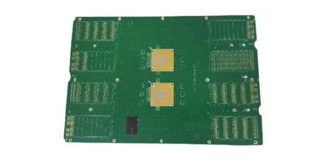
Different semiconductor testing environments require different PCB materials.
Common material options include:
High-Tg FR-4 Materials
Suitable for cost-effective applications requiring good mechanical reliability and thermal resistance.
Low-Loss Materials
Used for high-speed testing where signal loss and dielectric performance are critical.
Hybrid Stack-up Solutions
Applied in mixed-signal environments requiring a balance between cost, signal performance, and mechanical stability.
Proper material selection improves electrical consistency and long-term reliability.
Manufacturing Considerations for Reliable Load Board PCBs
Selecting the right manufacturing partner is important for achieving stable semiconductor test performance.
A capable load board PCB supplier should have experience with:
- High-layer-count PCB fabrication
- Controlled impedance manufacturing
- HDI and microvia technology
- High-precision drilling and registration
- Electrical testing and inspection
- Quick-turn engineering support
Early engineering involvement, including stack-up review and DFM analysis, can help identify potential risks before production.
Applications of Load Board PCBs
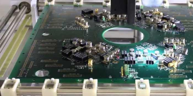
Load board PCBs are widely used in:
- Semiconductor final testing
- IC validation
- Automotive semiconductor testing
- Power device testing
- Consumer electronics chip testing
- Industrial semiconductor applications
Each application requires high repeatability, stable electrical performance, and long-term reliability.
Conclusion: Improving Semiconductor Test Reliability Through Better Load Board PCB Design
Load board PCB performance directly impacts semiconductor testing accuracy, production yield, and manufacturing efficiency.
By optimizing signal integrity, power delivery, thermal stability, mechanical reliability, and manufacturing precision, a well-designed load board PCB enables more consistent test results and improved production performance.
For semiconductor companies seeking reliable test solutions, choosing an experienced PCB manufacturing partner with strong engineering support is essential for achieving stable and scalable testing operations.
